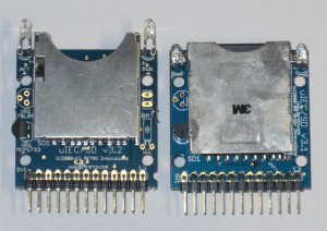
Even though there’s not much to tell, some folks asked about the differences in the new v3.2 uIEC/SD design. A picture is worth its weight in gold here, but I’ll also point out some less apparent details.
- Due to the new SD socket footprint, I was able to push the edge of the socket further from the edge of the board. This should help with implementations sitting behind thick plastic cases.
- Two small half moons (on the top left and bottom right) should allow the unit to be mounted in a Hammond 1551RBK enclosure.
- Although not populated on the PCB, there are pads for a Dallas DS1307 (or compatible) RTC with battery backup. The battery pins are shown on the right of the new PCB, while you can make out the watch crystal footprint below them on the right side.
- The LEDs have been pushed further outside the PCB. Truly, the assembly house went overboard on the first batch, but they should stick out to the edge of the SD socket.
Nothing else, I am afraid. I tried to add device jumpers to the design, but ran out of space and time to route the pads. The rest remains the sames, including:
- Pinout. v3.2 shares the same pinout as v3.1 and v3.0
- Mounting location. The mounting holes are in exactly the same place. Though the SD socket has mover 1/8″ further out, the PCB will fit in exactly the same place as previous designs.
- Same uC. The Atmel ATMEGA1281 is still in use, as is the 74LVC06 serial bus driver