Picking up from last time, we were able to successfully place a byte into the internal CoCo memory from the cartridge port without the use of the CPU by utilizing a direct memory transfer procedure. However, after the transfer, BASIC programs would stop with errors at times, machine language programs would simply lock up, and the IO registers of the cartridge device would be corrupted. Clearly, our initial implementation has issues. Since education and understanding drive this effort, we need to dig deeper into the actual bus activity. For that, we must turn to the digital logic designer’s tool of choice: the logic analyzer
For anyone who has even a passing interest in digital circuitry, I (and so many others) strongly recommend obtaining a 10-20MHz dual channel oscilloscope. A multimeter may be the first tool purchased, but an economical dual channel scope should be next on the list. That said, while oscilloscopes are great to see transients and strange signals (like NTSC or audio), they don’t handle digital logic investigation as well. Enter the logic analyzer. Instead of trying to replicate the shape of a signal like a scope, the LA simply detects whether a signal is 0 or 1 (typically using TTL voltage levels as a reference, where 0 = 0-0.8V, and 1= 2.1V-5V). It performs this limited action across many channels, as opposed to the 2 or 4 of a scope. After a scope, I strongly recommend obtaining a small 8-channel USB-based analyzer. They are inexpensive, easy to use, and 8 channels supports simple parallel testing and a plethora of serial protocol testing (RS232, SPI, I2C, etc.). That said, debugging a single board computer or large interface card can take a long time with 8 (or even 16 or 34) analyzer channels. Thus, I also keep a larger professional grade logic analyzer (it used to be the only option, before the USB analyzer options came on the market). Found on eBay from test equipment manufacturers like Tektronix and HP/Agilent/Keysight at reasonable pricing, these units support dozens and sometimes hundreds of analysis channels at frequencies far beyond what the 1980’s computer enthusiast will regularly see.
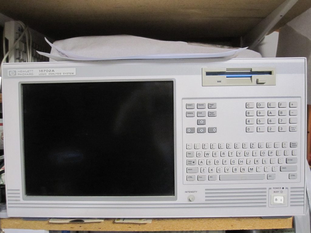
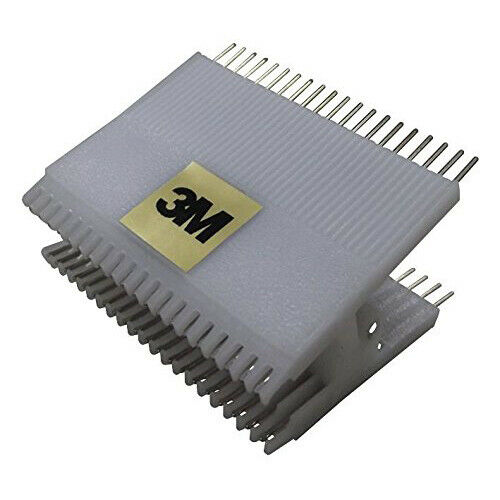
I’ve recently upgraded my bench analyzer from a 1980’s era HP 1650b (great unit, cheap to buy and own, now passed onto a fellow hardware designer to continue its usefulness) to a 2000’s era HP modular system (HP 16702a). This project gives me my first opportunity to learn how this unit works. I first connect the individual analyzer channels to the various 6809E signals using a 40-pin 3M Test Clip. I highly recommend adding this to your toolbox for signal inspection (the units are expensive if purchased new, but they never wear out, and eBay has more reasonable pricing), as they simplify moving the signal investigation to a new IC or new system. Since we want to investigate all of the bus activity, I place address lines 0-15 under test, as well as data lines 0-7, R/W (read/write), HALT, and the clock signals (E and Q). As we want to know what happens after the access of $ff61, we set a trigger on access to that memory location.
To more accurately pinpoint the issue, we’ll use a hastily (and terribly, I’ll add) written 6809 assembly application to exercise the test device and which exhibits the crashing behavior. A snippet is included below:
| … | |
| lda LOC | * grab initial data at $4000 |
| jsr CONVERT | * convert binary to hexadecimal and return in D |
| std SCREEN | * store at $0400 |
| lda DMA | * execute the DMA action ($ff61) |
| lda DATA | * grab data at $ff60 (the external IO data location) |
| jsr CONVERT | * convert binary to hexadecimal and return in D |
| std SCREEN+2 | * store at $0402 |
| lda LOC | * grab data at $4000 (the internal IO data location) |
| jsr CONVERT | * convert binary to hexadecimal and return in D |
| std SCREEN+4 | * store at $0404 |
| … |
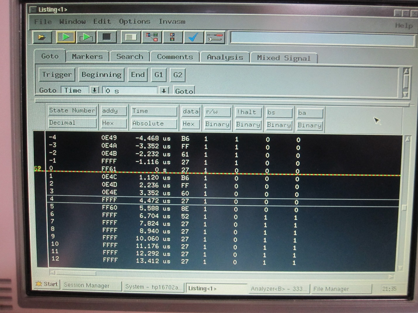
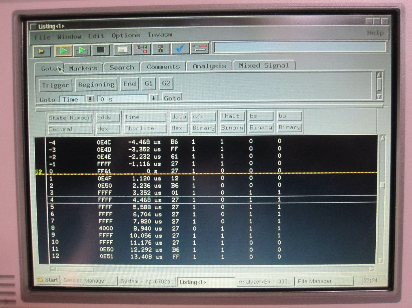
Since the application originates at $0e00, the lda DATA instruction after our $ff61 access resides at $0e4c. When we run the test program, the logic analyzer triggers and the program crashes. But, the evidence surfaces. On the logic analyzer, we see the following:
| Address | Data | R/W | HALT | Notes |
| 0e49 | b6 | 1 | 1 | |
| 0e4a | ff | 1 | 1 | |
| 0e4b | 61 | 1 | 1 | |
| ffff | 27 | 1 | 1 | Dead Cycle |
| ff61 | 27 | 1 | 0 | Nothing at $ff61, but bus rests at $27 |
| 4000 | 2d | 0 | 1 | Our data write ($2d = 45) |
| We sample on falling E, so HALT=1 | ||||
| 0e4d | ff | 1 | 1 | Why did we jump to $0e4d? |
Folks probably start to see what is going on, but it pays to be sure. The Verilog is modified to not activate the address bus or R/W line, hold HALT low forever, and the test is repeated. Here is the result:
The problem begins to show itself. Even though the device has pulled HALT low before the end of the instruction execution, the CPU reads and executes one more instruction before releasing the bus. We can tell because of the state of the BS and BA lines. The 6809 datasheet notes that BS=BA=1 signifies a HALT condition in the CPU. Further attempts to pull HALT low earlier in the $ff61 read cycle make no difference.
Darren Atkinson (of CoCoSDC design fame) emailed after hearing about the project effort, asking about HALT line triggering. I initially misread his email as inquiring whether I had pulled HALT low early enough in the instruction cycle. But, Darren responded again and pointed to a key portion of the datasheet I had misinterpreted:
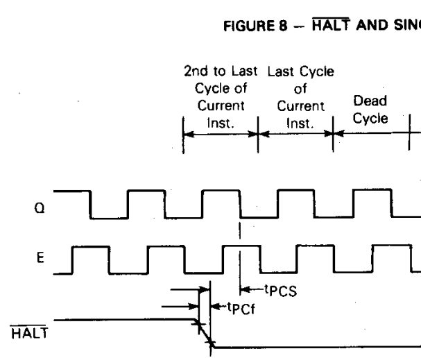
Hint: It’s the text at the top of the page. I noticed the “2nd to Last Cycle of Current Instruction” notation, but interpreted it to be illustrating to the reader that activating the HALT line before the last cycle of an instruction would not cause an immediate reaction. From my days working with the 6502, I knew that 8-bit processors are not designed to maintain an intermediate instruction state for any length of time. The CPU assumes that once an instruction is started, it must complete before anything else will be processed. While this doesn’t seem to be a concern for the HALT condition (just simply stop the processor, wait for HALT to become inactive, and continue on), it makes sense that HALT would use the same sense logic and internal handling logic as interrupts, and stopping the CPU in mid-instruction to handle an interrupt would require saving an intermediate instruction state. Thus, for that reason, the simpler 8-bit CPUs just don’t do that. Once an instruction opcode is fetched, the CPU will fully execute the current instruction before handling any event. If the datasheet showed the HALT line going low on the last cycle, it could imply that execution would stop at the end of the current instruction cycle. Thus, I thought this text was simply reinforcing the text describing the HALT pin: “A low level on this input pin will cause the MPU to stop running at the end of the present instruction and remain halted indefinitely without loss of data”.
However, my assessment was plain wrong. As Darren pointed out, the “2nd to last instruction” text carries crucial significance. As well, it’s the key to the problem we are experiencing. The Verilog is activating HALT on the last cycle of the current instruction, which is actually too late. The CPU moves ahead to read and process the next instruction, only then latching and acting on the HALT condition. I wish this prerequisite had been noted somewhere in the datasheet, but I checked the 6809E, the 6809, the 63C09E and the 63C09 datasheets online and in my possession and found no mention of the constraint. That said, a Facebook commenter also pointed out this requirement, so perhaps everyone in CoCo land knows this tidbit of information.
Now that we know the issue, how do we solve it? I first added a NOP to the code, thinking that doing so would allow the next real instruction to be read correct (the lda $ff60). However, before testing, I quickly realized that would not work. Since the CPU is still reading an opcode, it would interpret any data on the databus during that cycle as the next opcode, potentially altering the program anyway. I next added Verilog code to wait an arbitrary 8 cycles after HALT activation before accessing memory:
- The read from $ff61 happens, and HALT is activated
- A NOP is read
- The next instruction is read (the second cycle of a NOP instruction appears to read and discard the next opcode)
- Then the CPU is halted (as shown by the BS=BA=1 condition
- The Verilog waits a few more cycles (shown as $ffff:$27 read cycles)
- Then the data is transferred to 4000 (in this test, the written value was $27) while HALT is deactivated.
- The CPU takes a cycle to acknowledge the deactivation
- The CPU takes another cycle to prepare for startup
- Then, the $b6 opcode (of lda $ff60 instruction) is read
Success! BASIC test applications begin running to completion with no unexpected errors, and the test machine language application no longer crashes the machine, instead it runs to completion and illustrates that all 256 values can be transferred from outside the machine to internal memory locations.
That said, adding dead cycles to the DMA engine is far from ideal. In fact, after Darren noted that a full register stack-up could take 20+ cycles on a 63C09, I quickly found the dead cycle wait idea untenable. Clearly, we need to find a better way to trigger a DMA transfer. I quickly sketched out a few requirements and some preferences:
- The action must pull HALT low prior to the second to last instruction cycle
- The condition must not occur over two consecutive opcodes (interrupt could occur in between)
- The condition must not require scanning the databus for specific opcode/operand sequences (i.e. watch the databus for $b6,$ff,$61)
- Doing so requires constantly activating the SLENB line when installed in an MPI, since the data bus is hidden from MPI slots unless an IO access is made or SLENB is activated. And, SLENB being activated on arbitrary memory locations would cause other problems
- There’s no guarantee such a sequence would never occur in any other way.
- Ideally, the “trigger” action should be an instruction that would be otherwise needed (so as to not waste any time performing some action JUST to start the transfer)
- If a memory address trigger, the address should be constant
I just as quickly decided that CPU instructions that perform 2 memory accesses in a single instruction would ideally suit these constraints. HALT could be triggered to go low on the first memory access, and if the second memory access did not occur 1 or 2 cycles later, the HALT condition would become inactive and the system would not perform the transfer. If the condition was met, the system initiate a transfer after the second memory access. I first gravitated to INC $ff61, which performs a ®ead-(M)odify-(W)rite action (reading the memory location, adding 1 to the value, and writing it back to memory). Since INC $ff61 performs a read cycle, then takes an internal cycle to perform arithmetic (ALU) operations, and finally writes the new value back, the Verilog state engine needed to detect the initial access, wait a cycle, and then detect the second access. That’s not hard to support, but it’s wasteful. Supporting preference #4 proves the larger challenge. Rarely would someone need to increment a value in the DMA engine register set. While I was debating options, fellow enthusiast and Nitros9 developer L. Curtis Boyle suggested LDD, which performs 2 consecutive memory accesses in 2 consecutive cycles. While LDD may not be of great use, STD (store D) would often be used to place a 16 bit value in the registers, as would other 16-bit memory store operations. Since it also simplifies the Verilog, we will utilize it as the DMA transfer start mechanism. In essence:
- Once the lower IO register is accessed, bring HALT low and set flags
- In the immediate next cycle:
- If the next higher IO address is accessed in the next cycle, continue to hold HALT low and prepare for a DMA transfer
- If not, release the HALT line and do not prepare for a DMA transfer
If the first condition is met but not the second, the CPU will likely notice the HALT condition and stall for 2 cycles after the current instruction, but no harm will arise. To prevent accidental DMA activity while setting register values, we should also add a bit in the eventual control register to enable or disable DMA transfers.
More testing is needed to understand other issues, if any, with assuming a transfer can begin immediately following an LDD/STD type instruction. Since Darren Atkinson already broached the subject of interrupt handling, he performed a test that activated NMI and HALT at the same time, attempting to understand which behavior took precedence. Darren utilized the following circuit and program snippet:
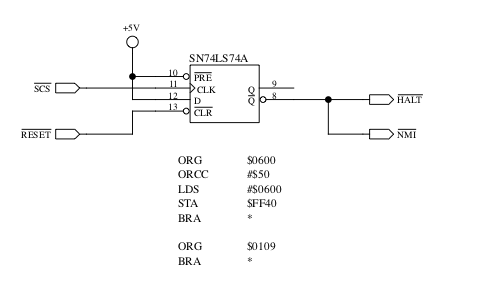
By organizing the stack right above screen memory and driving NMI and HALT low with an SCS access to $ff40, NMI precedence would show as characters on screen (stack values). When executed, no such values appeared, which strongly suggests HALT takes precedence over interrupts.
Now that we have verified the ability to safely transfer data from outside the CoCo to internal memory without disrupting program execution and a way to reliably and atomically trigger such a transfer, we will put all of the pieces together into action. Many thanks to those following along on this journey so far, and a special thanks to Mr. Atkinson for his insights.