With the introduction of the TANDY Color Computer (CoCo) 3, engineers were faced with 2 significant and implied mutually exclusive goals:
- Design a worthwhile successor to the venerable CoCo 1 and 2, enhancing the capabilities of the machine in non trivial ways that would create a competitive solution in the new crowded marketplace while still maintaining compatibility with the previous generations, and
- Hit a key low price point, to allow sales with 8 bit home computing systems being squeezed from 16 bit machines in the top end and reduced cost older platforms taking up the low end of the marketplace.
To satisfy both of these goals, the CoCo 3 consolidated the MC6883/74LS783 Synchronous Address Multiplexer (SAM) and the MC6847 Video Display Generator (VDG) into a single Application Specific integrated Circuit (ASIC) while adding additional graphics capabilities. Officially called the Advanced Color Video Chip (ACVC), the TCC1014 (VC2645QC) IC does much more than increase video functionality for the CoCo 3. As such, it’s rarely called the ACVC, but rather the Graphics, Interrupt, Memory Enhancement, or GIME.
Though the video enhancements rightly get their due, the memory expansion is also of interest. The CoCo3 has some of the most advanced memory functionality of any low cost home computer of its time period. Not only does the system offer 512kB of RAM usage, but it offers a powerful way to utilize all of that RAM within the constraints of the 64kB directly addressable memory space dictated by the Motorola MC6809E CPU.
While doing research for a recent presentation, I wanted to revisit an interesting piece of trivia I first learned about in 2016 as I worked to expand my CoCo 3 beyond 512kB. While probing the memory addressing, I noticed something strange about how memory was accessed in the CoCo 3.
The CoCo 3 utilized dynamic random access memory (DRAM), which was accessed via a multiplexed address bus. Thus, unlike the more traditional static RAM (SRAM) which could connect directly to a CPU address bus, DRAM required the address be sent in two parts, a “row” and a “column”, using signals called the Row Address Strobe (RAS) and Column Address Strobe (CAS). This reduced IC size, which reduced IC cost, important as systems tried to offer more RAM.
As hardware developers know, the address lines on an SRAM IC are mere suggestions, as one memory location is as good as another. Thus, even though an SRAM might have address lines 0 to 12, there’s no requirement they be connected to the CPU address lines 0 to 12 in the same order. Some designs used that to simplify PCB trace routing. DRAM shares much of the same flexibility. There are some requirements around accessing all memory “rows” every 4 or 8 milliseconds to ensure the DRAM capacitors remain charged, but any address line can be sent in any order as long as half are sent during the RAS part of the cycle and half on the CAS part of the cycle.
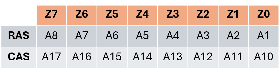
That said, most designs place the lowest address lines in order on the multiplexed address bus during the RAS portion of the memory cycle, while the higher address lines are sent in order during the CAS portion. Thus, when I probed the 9 CoCo 3 memory address lines, I expected to see the following:
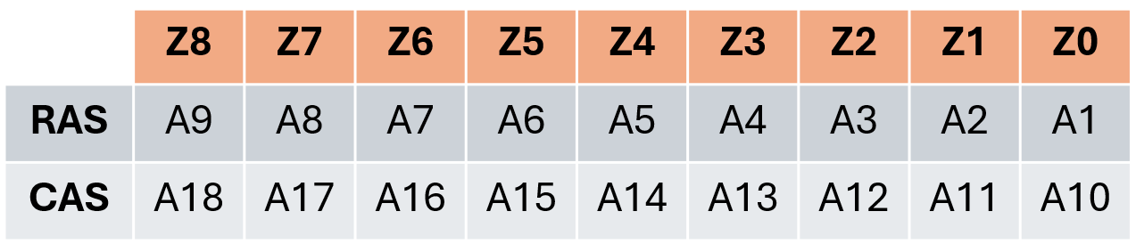
A0 is not included since the CoCo 3 has 2 banks of DRAM and the lowest address bit is used to select which bank will be read.
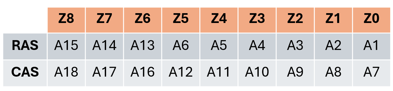
The probe data did not fit the above, so I thought perhaps the GIME spread the MMU-configurable address lines A18-A13 across the two strobe cycles, like so:
But, that also did not fit. Finally, I figured out the mapping:
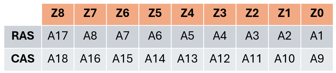
The next to highest address is sent on Z8 during RAS, while the highest address lines is sent on Z8 during CAS.
In 2016, I documented my findings and did not pursue the reasons further, but during my recent research, I decided to validate my earlier findings (they were correct) and consider why the address lines were jumbled like this. I noticed both address lines were sent on multiplexed address line Z8, the highest order line. I initially theorized that either:
- The GIME spent most of its design cycle as a 128kB capable design, with the 2 highest address lines added late in cycle.
- TANDY engineers were gravely concerned ASIC would not allow full 512kB addressing, so “pre”-re-ordered lines to make cutting down to 128kB design simpler.
After researching further, I realize the answer is much simpler. The GIME needed to support 2 memory sizes, 128kB and 512kB. Supporting 512kB required all of the address lines, but supporting 128kB only requires address lines up to A16. If A16-1 were arranged on the lowest lines (Z7-0) of the multiplexed address bus, commodity 64K DRAMS supporting only multiplexed address lines Z7-0 could be used without additional circuitry (the GIME always takes care of selecting the bank using A0). Specifically, mapping the GIME address lines Z7-0 to the standard 4464 64kb x 4 bit DRAMs installed on the CoCo3 yields the following:
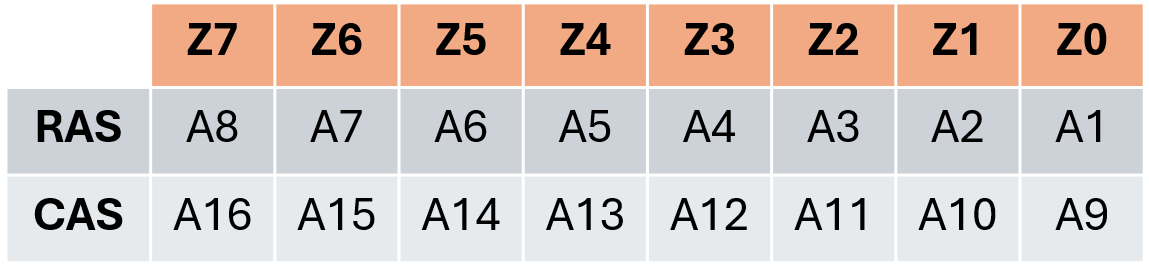
Notice address lines A16-1 are sent to the DRAM inputs Z7-0. On the other hand, putting address line A9 on Z8 during the RAS cycle (as in the first mapping) would cause memory repeat issues:
The first 512 bytes of memory would be fine, but then address 512 ($0200), in which A9=1, would be seen as $0000 by the memory, and this issue would repeat every 1kB.
I thought I’d found some callback to the original GIME design process, but the design is impressive nonetheless. TANDY engineers ordered the address lines to support two different memory configurations in an elegant and cost effective way.