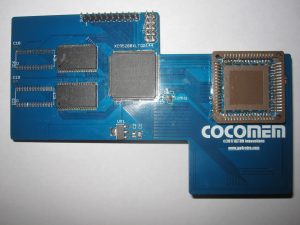
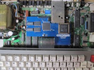
 Introduction
The TANDY Color Computer 3 married the elegance of the Motorola 6809 microprocessor with a simple but powerful memory management system breaking the 64kB barrier. The original system offered expansion options up to 512kB, and the OS-9 operating system, among other applications, was enhanced to support the additional memory capacity.
Memory expansion could be performed by the end user, utilizing on-board connections for attachment, but the process was deceptively complex. The end user must remove existing system RAM, slightly modify the system board by removing two electronic components (or rendering them non operational) before inserting the memory expansion unit. This made it more difficult to return the unit to a stock configuration, for later use and/or sale.
In addition, the on-board expansion capabilities did not support expansion options greater than 512kB. Over the years, 2 megabyte expansion solutions were developed and sold, requiring even more complex installation instructions (some required unsoldering the microprocessor, soldering in a socket, installing multiple circuit boards, possibly in addition to the steps required for the 512kB memory expansion. Probably due to their complexity, these memory expansion solutions saw limited release, and the companies producing these solutions are no more.
Though newer Color Computer hardware manufacturers now provide easily installed 512kB memory expansion options, there continues to be a need for larger memory expansion solutions. However, new offerings must address the ease of installation concerns the plagued older product offerings.
Any new system must:
- Offer significant memory expansion capability (2MB at minimum)
- Work with existing software that does not understand the larger memory capability
- Require no or very little modification of the Color Computer 3
- Utilize very little power
- Produce very little heat
It should also:
- Allow existing memory to be left in place
- Support returning the system back to a stock configuration, for problem determination, sale, or migration to a new system
- Support earlier memory expansion configuration capabilities, to allow use of existing applications
With these concerns in mind, we would like to introduce RETRO Innovations’ CocoMEM Color Computer memory expansion system, the simple no-solder premier memory expansion system for the TANDY Color Computer 3.
 The CocoMEM memory expansion system for the Color Computer 3 comprises a single circuit board that plugs into the Coco3 GIME socket, with the GIME IC plugged into the CocoMEM circuit board. This allows the circuit board to capture all signals needed for complete MMU functionality without requiring any irreversible modification to the Coco3. To remove, simply remove CocoMEM and replace the GIME in the original socket. Existing memory in the Coco3 can be left in place (feel free to remove if desired), and no capacitors must be clipped or otherwise removed. No additional installation effort is required
The CocoMEM design supports the following features:
- Hardware support for 64 MB of system RAM (test units have 4MB installed)
- 16 bit task registers
- Dual MMU support (Separate registers for video MMU and CPU MMU)
- Map video MMU registers to any 512kB bank in memory
- Support for 32 CPU MMU tasks, each with their own set of task registers
- Support for 256 CPU MMU “tasklets” per task, each with their own set of task registers
- 512kB “emulation” mode (on Barry Nelson’s request)
- NoCan3 $ff9b bank register support
Additional immediately planned features:
- Per task bank write protect capability
- Per task bank CPU read interrupt
- Per task bank CPU write interrupt
- Map any GIME MMU register to any 8K bank in memory, no 512kB segment restriction
Options
Requirements
- Tandy Color Computer 3
CocoMEM units are currently in development, but will be sold in the RETRO Innovations Online Store.
Units come with a 30 days return policy and 1 year warranty.
Technical Details
CocoMEM generates the bulk of its simplicity and power by residing in the GIME socket, which manages all traffic in the TANDY Color Computer 3. All CPU, video, and RAM traffic runs through this single socket, and it is one of the very few ICs socketed on on the Coco3. By intercepting all CPU and GIME traffic, the unit can alter the behavior of the system.
In a normal Coco3, the GIME generates both system clocks (E and Q), and manages all read access to RAM and part of the CPU’s write access to RAM. The GIME accesses memory in 16 bit amounts, but presents an 8 bit data bus to memory.
- During a video memory read access, 16 bits of data are read from memory, 8 bits of which is sent immediately to the GIME, and 8 bits are saved to be sent while the CPU is accessing memory.
- During a CPU memory read access, 16 bits of data are sent to the GIME, which then selects which byte of the word (high or low) should be returned to the CPU
- During a CPU memory write access, the GIME selects which bank of RAM (high or low) will be sent the 8 bits of CPU data and strobes the write enable line of the respective memory bank.
CocoMEM intercepts GIME video data accesses, replicating the “16-to-8” marshalling login on the Coco3 motherboard to present appropriate data to the GIME
However, for CPU memory accesses, CocoMEM does not pass the data through the GIME, instead directing memory reads and writes directing to/from the CPU.
This allows the system to separate GIME MMU registers from CPU MMU registers. It also allows more efficient use of the CPU cycle, as newer static RAM does not require 250nS of time to read or write data. Thus, 2 banks of RAM are connected on CocoMEM. One, a larger block of RAM, is used for data storage. The other, a smaller 64kB block of RAM, is used to hold MMU register values.
Video memory access occurs on the low half of the E cycle. CPU access is performed on the high half of the E cycle. On CocoMEM, the high half of the E cycle is further divided into 2 parts: MMU access and data access. In the first part of the high E cycle, the MMU address is presented on the address lines, the MMU RAM is enabled, and 16 bits of MMU data is latched into internal registers. Then, on the second portion of the cycle, main RAM is enabled, the address lines change to reflect MMU and CPU address values, and the appropriate bank of RAM is interfaced with the CPU.
- To support emulation, bit 7 of GIME register $ff90 is utilized (0 is native mode, 1 is emulation)
- The task register at $ff91 is extended to 5 bits, enabling 32 tasks
- Bits 0 and 1 of location $ff96 alters the data “window” present at the $ffax MMU registers:
- 00 (default). GIME and CPU registers are both written by any write access to $ffax. GIME registers continue to be 6 bits, while the bottom 8 bits of the task register reflects the value at $ffax. The high byte of the CPU MMU register is written with the value at $ff9b on any write access (normally 0). Reads will return the 8 bits of the CPU MMU register’s low byte
- 01: GIME registers are shows at $ffax
- 10: CPU MMU register bits 0-7 are shown at $ffax. A write only updates the CPU MMU register’s lower 8 bits.
- 11: CPU MMU register bits 8-15 are shown at $ffax. A write only updates the CPU MMU register’s upper 8 bits.
- $ff97 is utilized to support 256 tasklets
- $ff9b emulates the NoCan3 MMU configuration register, though this is only provided for compatibility and cannot be utilized to support more than 16MB
The system currently comprises 5 ICs:
1 Xilinx XC95288XL-144
2 AS6C1608 16Mb x 8 55nS static RAM
2 IS61LV256-12 256kb x 8 12nS static RAM