CoCo DMA: All Charged Up!

Addressing the Color Computer 3 DMA operation challenges via hardware modification, while pretty simple, limits initial adoption. It places the technique into a classic “chicken and egg” situation. The CoCo3 provides an ideal platform for DMA capabilities, but owners will only perform hardware modification if highly desired peripheral capability demands it. Hardware designers, for their part, prefer to focus energy on innovative peripheral design that targets common CoCo3 hardware configurations. What if we could shortcut the process by implementing a solution that does not require hardware alteration?

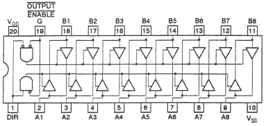
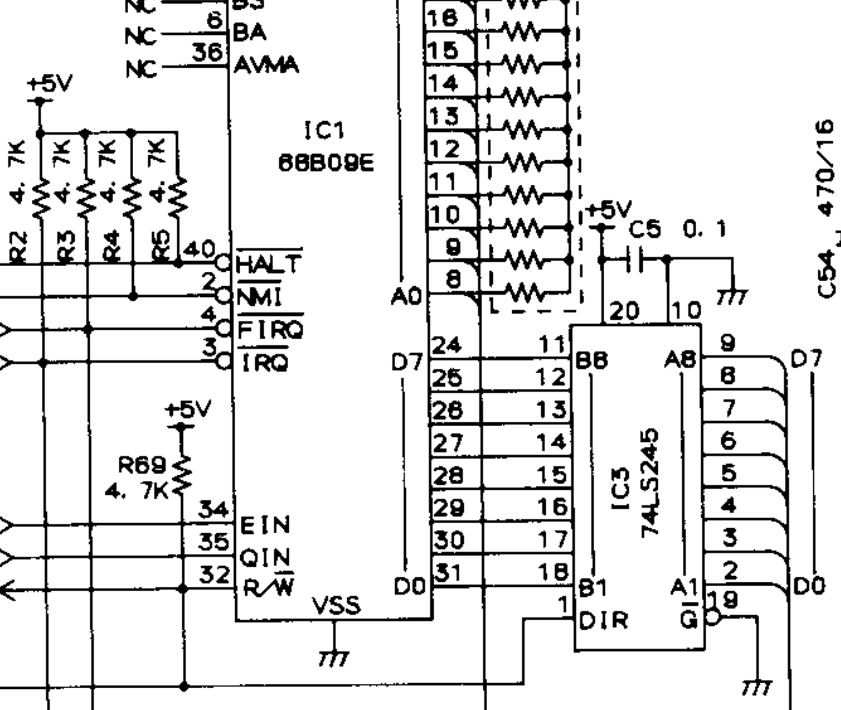
Return your attention to the portion of the schematic showing the M68B09E data bus and the 74LS245 bus transceiver, the root of the challenge. As we have noted, the transceiver is always tied to the memory data bus (pins 2-9 in the schematic) and outputs data onto the memory bus during any write cycle. How might we work around this constraint or, failing that, leverage this fact? One idea often considered attempts to “race” the ‘245 transceiver. Essentially, place the data you want to store on the bus, delay issuing the write until the last possible moment, enable the write line, which then enables the ‘245 buffer, and then hope that the memory latches your data before the ‘245 flips over and places its data on the bus.

Figure 1: CoCo3 CPU Data Bus Schematic

First, let’s review DRAM access by referencing the timing diagram for a Texas Instruments 4464 64kbx4 Dynamic Random Access Memory (DRAM) in Figure 2, of the same type often installed in the CoCo3. For various reasons (pin count reduction, moving the multiplexing function out of each IC into a common area, supporting faster memory access options), DRAMs expose multiplexed addressing pins. Think of a DRAM as a matrix of memory cells arranged in a row/column configuration. To read or write DRAM memory, one places the row portion of the address onto the multiplexed address lines, and activates the “row address strobe” (CAS) signal. The DRAM latches the row value and calls up that row in the memory matrix. A short time later, one places the column portion of the address onto the same pins and activates the “column address strobe” (CAS) signal. The DRAM then reads or writes that portion of the matrix.

Figure 2: DRAM Write Timing

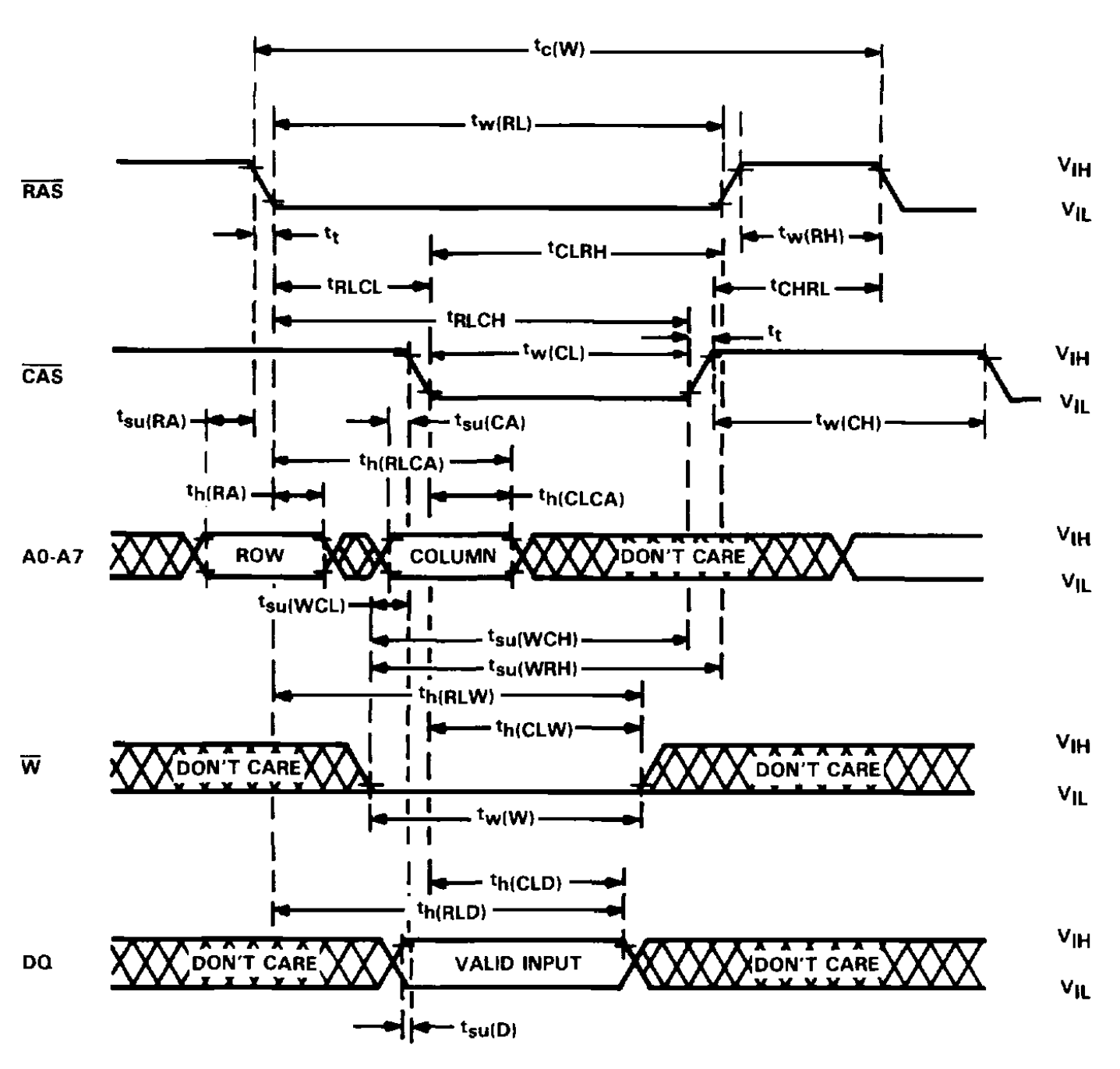
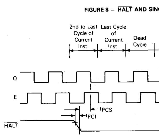
There are rules to follow. Notice the “write” signal, denoted by a W with a line over it (active low). Right above it and below it, focus attention on the arrows showing th(CLW) and tw(W). th(CLW) illustrates the amount of time after the CAS line falls until the write line can go inactive (essentially, the time it takes for the actual memory write to occur). Tw(W) illustrates the duration the write signal must be held low. For a 150nS (nanosecond) speed grade DRAM, Tw(W) and th(CLW) are both specified as 45nS minimum (the timing diagram misleadingly suggests the write line must be pulled low before CAS goes low, which is not true).

On a CoCo3 running in FAST mode, we have ~280nS to perform a CPU write (560nS for a complete cycle at 1.78MHz, and the CPU gets half of that). Assuming the write will complete at the end of the CPU cycle, that means we need to enable the write function 45 nS before that, or at 235nS. This poses a problem. Assuming that the address starts getting set up at the beginning of the CPU portion of the clock cycle and we don’t immediately activate the write line, the DRAM will perform a read activity, culminating in valid data on the DRAM data lines 150nS after the start of the cycle. We weren’t going to activate the write line until 235nS into the cycle, so now the data on the memory bus (from the DRAM) will be fighting the data we’ve placed on the bus. If that isn’t enough of an issue, when we activate the write line, the 74LS245 will enable data on its output lines approximately 25nS after doing so. But, we need stable data for 45nS after activating the write line. The good news is that we’re no longer fighting the DRAM on the bus, but we end up fighting the ‘245 on the bus for 20nS before the end of the cycle (45ns – 25ns).

Perhaps, if we choose not to fight the 74LS245, we may be able to leverage it do help our cause. Enter Darren Atkinson once again. While I was preparing and testing the hardware solution for this challenge, Darren (who had started conversing with me on the topic some weeks ago) started considering options and dropped a deceivingly simple email to me on the topic a week ago. Between us, we have refined this idea, which I now present to the public on behalf of Darren and myself.

The essential idea: We can’t keep the 74LS245 off the memory bus during a write cycle, but what if we can leverage it to put the data we want onto the bus?

Let’s illustrate the CoCo1/2/Dragon timing diagram. I should take moment here to sing the praises of the WaveDrom (https://wavedrom.com) Online Timing Diagram Editor:

Figure 3: CoCo1/2 DMA Write Example

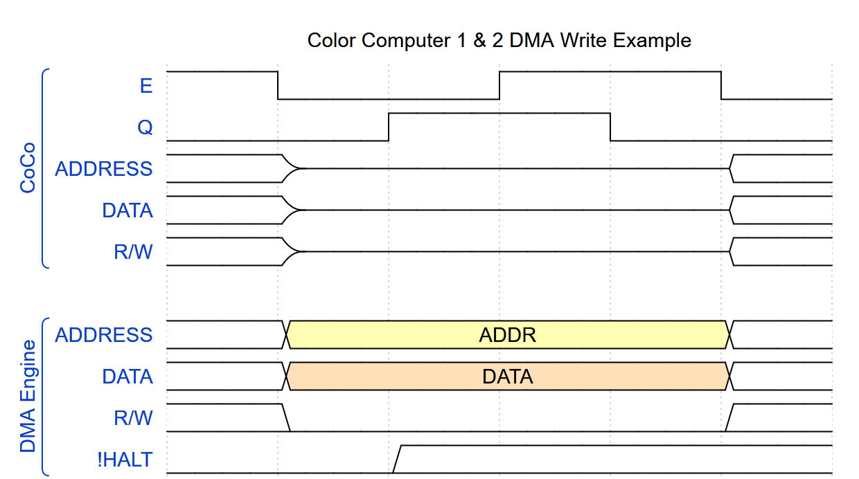
Shown here, the address and data lines are activated by the DMA engine during the entire computer cycle, along with the enabled R/W line. The CPU essentially removes itself from the bus during the cycle. If we consider the Color Computer 3, we know from Figure 1 that the 74LS245 will output data onto the bus during a write cycle, but we also know that the memory is not connected to the CPU during the first half of the cycle (the GIME accesses memory during this time). What if we could store a value on the one side of the ‘245 during the first part of the clock cycle, and then have the transceiver push that value onto the bus during the latter half of the cycle? That would be awesome, except the only thing connected to the other side of the bus transceiver is the CPU, now removed from the bus, and some short PCB traces. It doesn’t look too promising.

Since you know where this is going, let’s dig a bit deeper into electronics. In hardware design, we like to think of computers as digital systems, where the only thing that matters is high or low, 1 or 0, +5Volt or ground. That’s great, but digital computers are inherently analog in nature, regardless of how much we want to ignore that. In analog circuits, everything has an inherent capacitance, or the ability to hold a voltage charge for a period of time. As well, everything has an inherent resistance, or a desire to slow down the flow of electrons. In fact, this capacitance and resistance lies at the heart of DRAM. Unlike static ram, where the memory cell holds its value until power disappears, a DRAM cell is basically a small capacitor, holding a bit of charge (or not) that represents the value desired in that memory bit location. The inherent resistance in the DRAM cell slowly “bleeds” off the voltage in the capacitor, which is why DRAM must be “refreshed” every so often. Delay the refresh, the resistor bleeds off too much charge, and the memory is lost.

What if we treat the external pins of the CPU data bus, the small traces between it and the 74LS245, and the connected pins of the bus transceiver as a set of 8 small memory cells? They are crude and they will lose their value very fast, but perhaps they will hold a value long enough for us to accomplish our goals.

Let’s revise our timing diagram with this idea. Instead of placing data on the data bus for the entire cycle, let’s place data onto the bus during the first quarter of the cycle, while we also hold the read line high. With the CPU tri-stated (though the CPU pins are still physically connected to the bus, and so can participate in our memory cell idea), the bus transceiver dutifully captures that data and places it onto the now tri-stated data pins of the CPU (and the traces between the bus transceiver and the CPU). Then, a quarter cycle later, the DMA engine pulls the data off the bus, and signals the system to write data, placing the correct address onto the address bus that time as well. At this point, the 74LS245 bus transceiver should dutifully read the CPU data bus pins, which now hold the residual charge placed there moments before. The transceiver, locked into the “write” mode, will then amplify that charge and place it onto the memory bus, where the DRAM can access it.

Figure 4: No-Mod CoCo3 DMA Timing Diagram

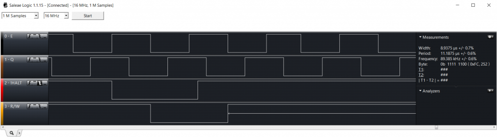
Outcome: Success! It turns out that our little 8 bit memory cell can charge up in 140nS or less and will hold its value for at least 840nS (3/4 of a cycle in SLOW mode).

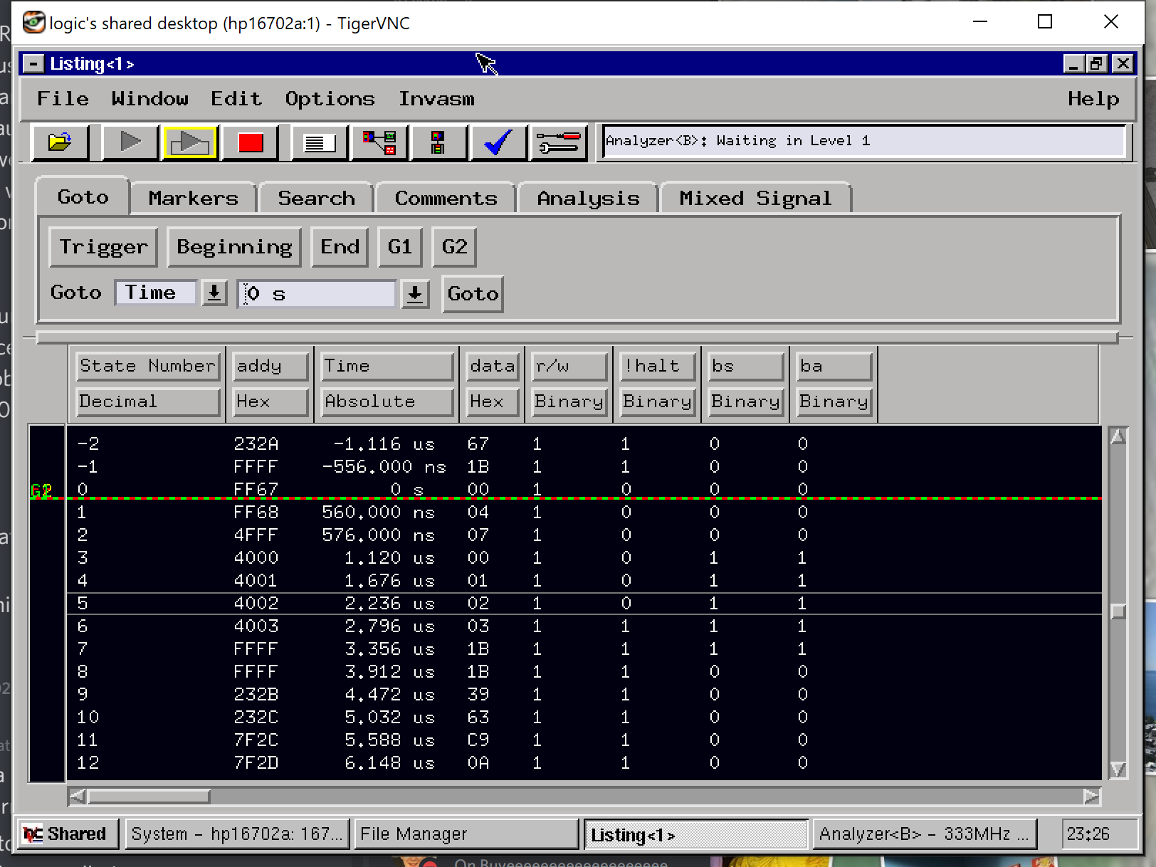
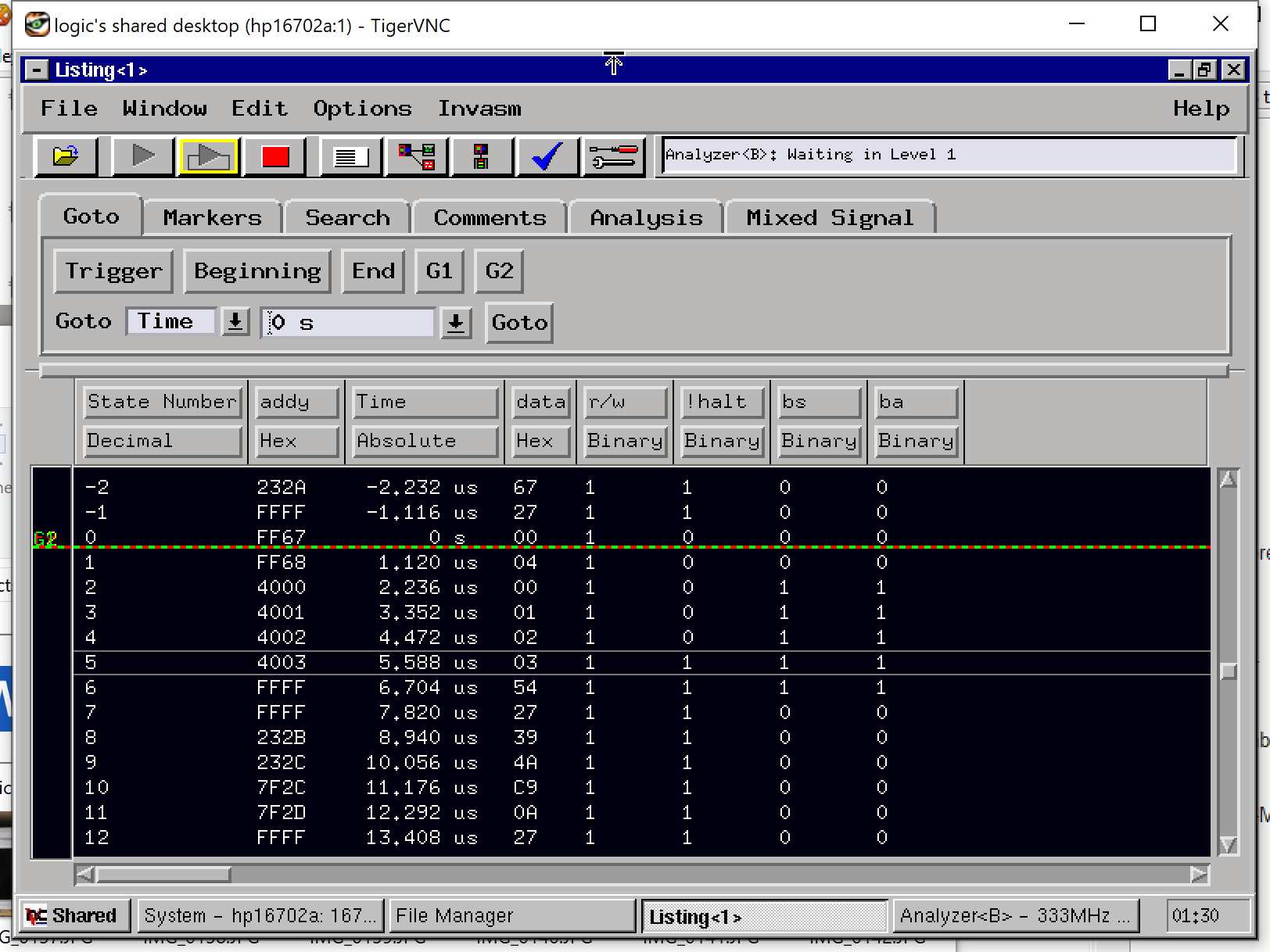
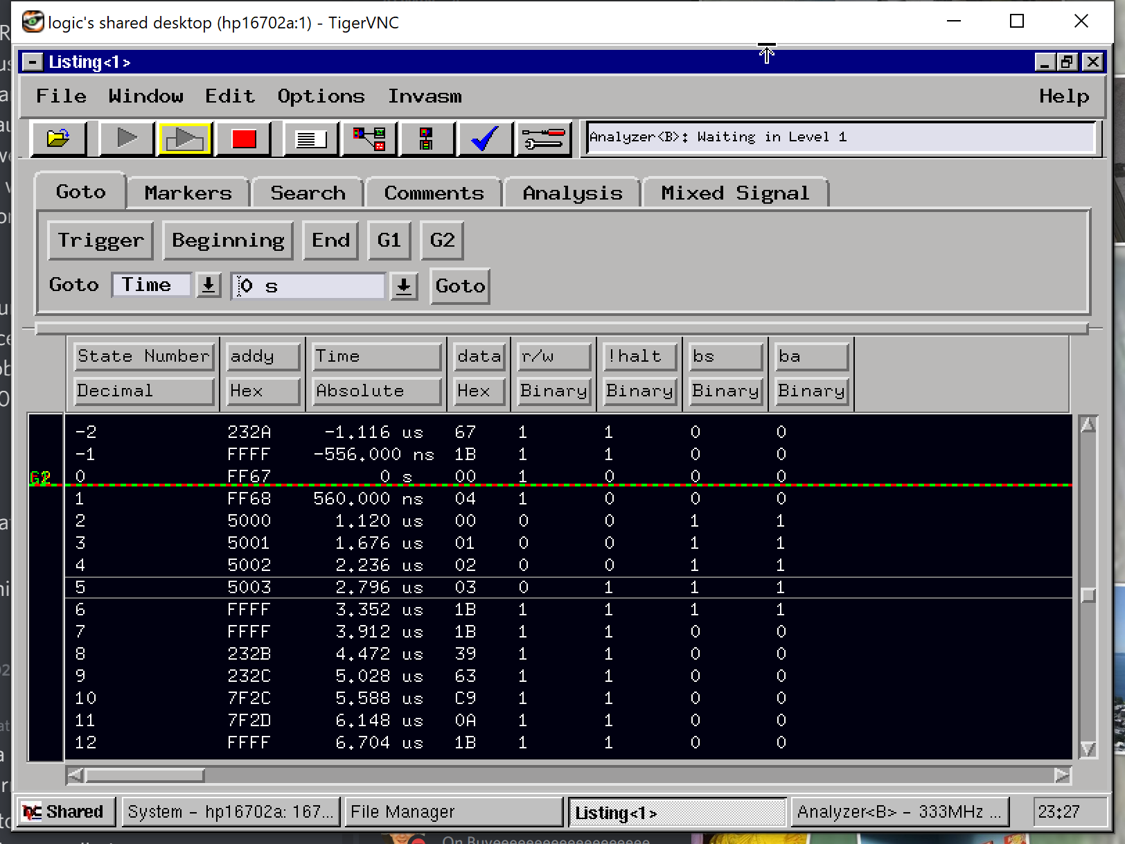
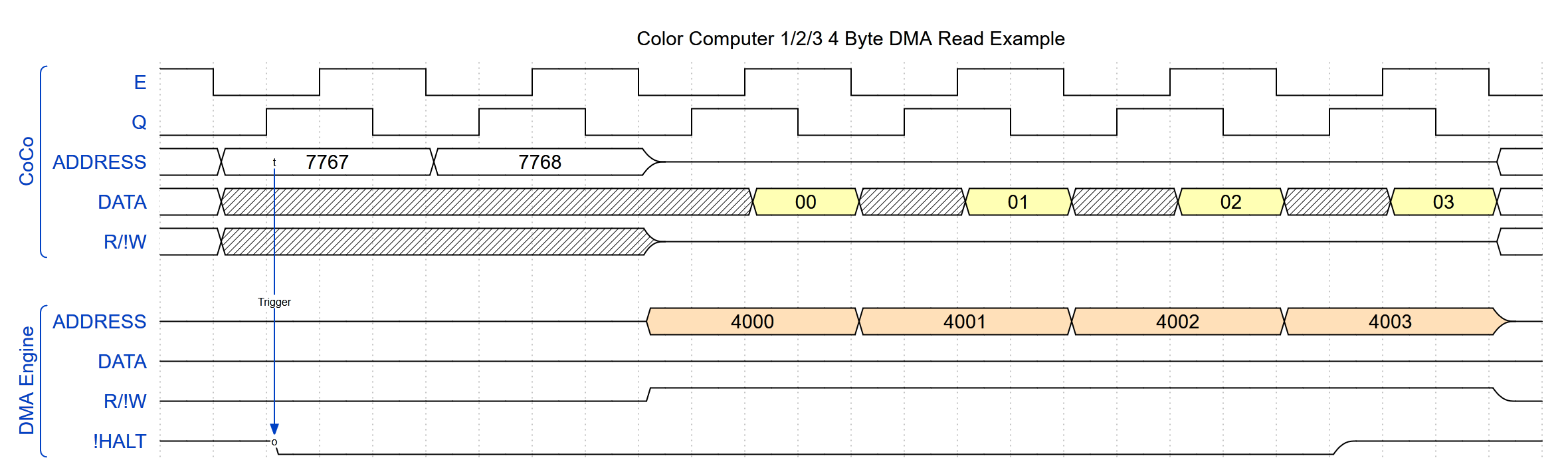
Let’s step back and look at the entire DMA process, both for reads and also for writes, with special emphasis on the changes needed for the CoCo3. As you will recall, all Color Computers share the same read operations, placing the system into DMA mode and reading memory:

Figure : Color Computer 4-Byte DMA Read Example

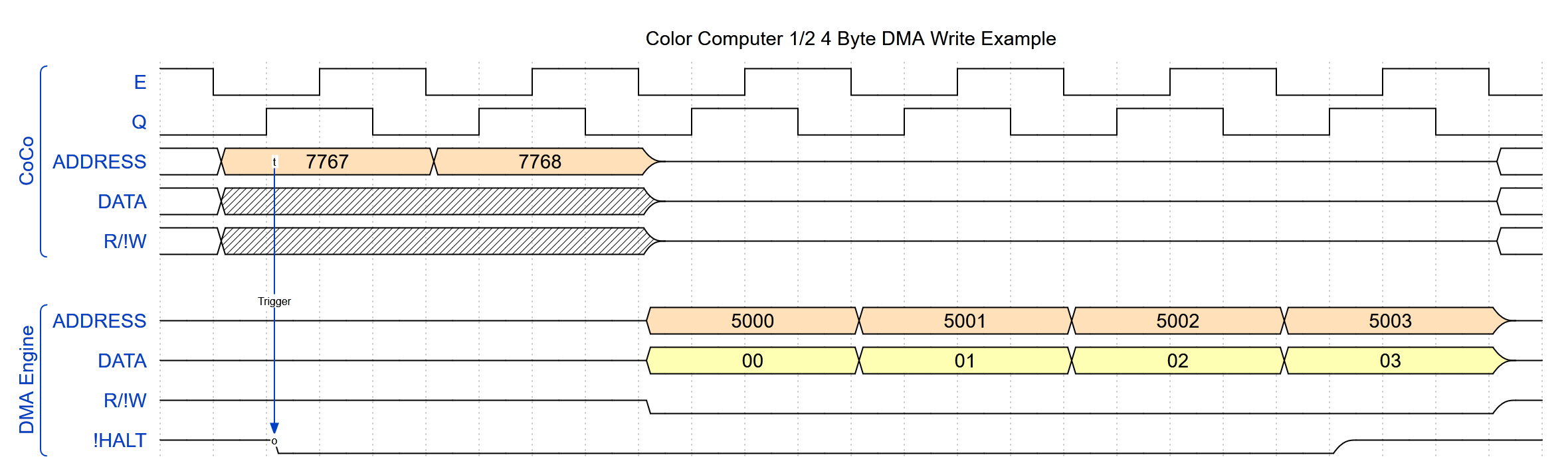
For DMA write operations on the CoCo 1 and 2, things change very little. We place data on the data bus and signal a write to memory:

Figure : Color Computer 1 and 2 4-Byte DMA Write Example

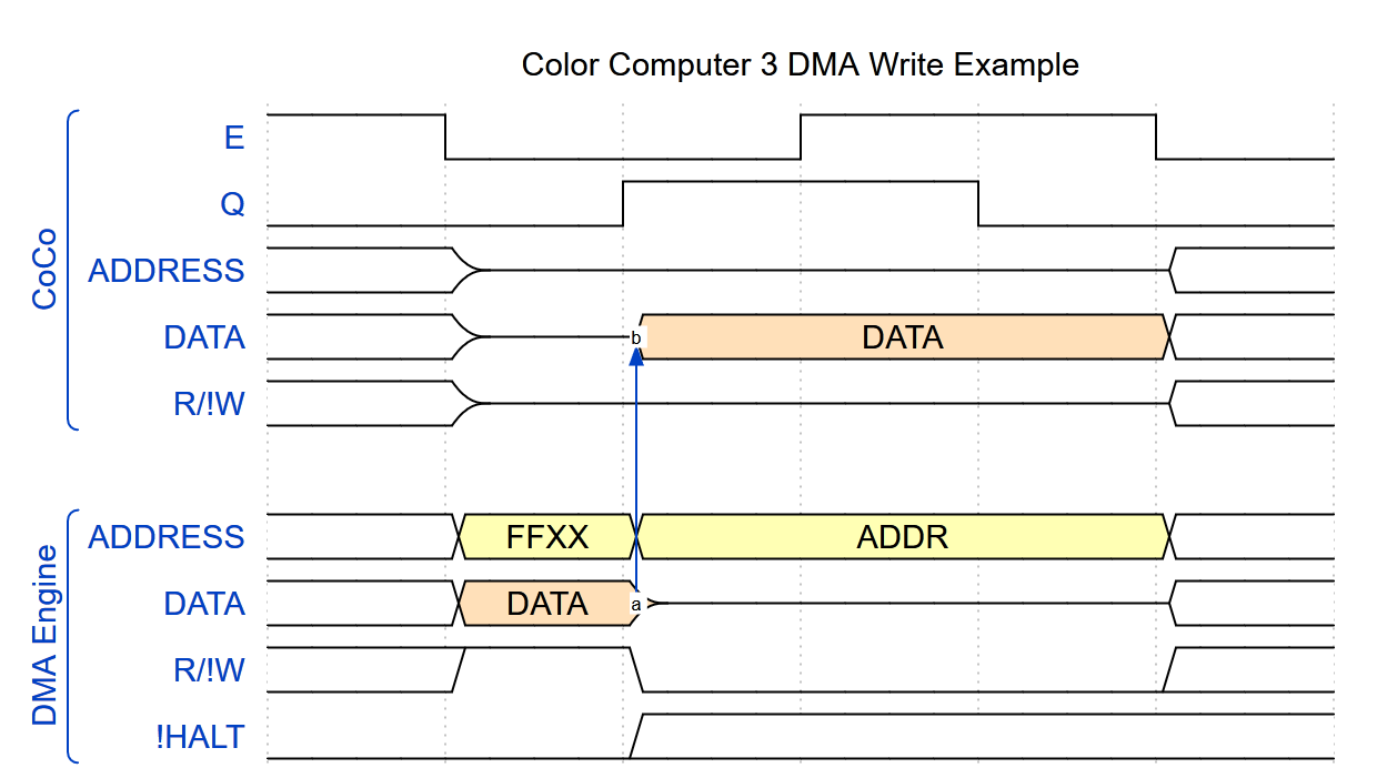
Finally, let’s show how this changes slightly to accommodate the CoCo3:

Figure : Color Computer 3 4-Byte DMA Write Example

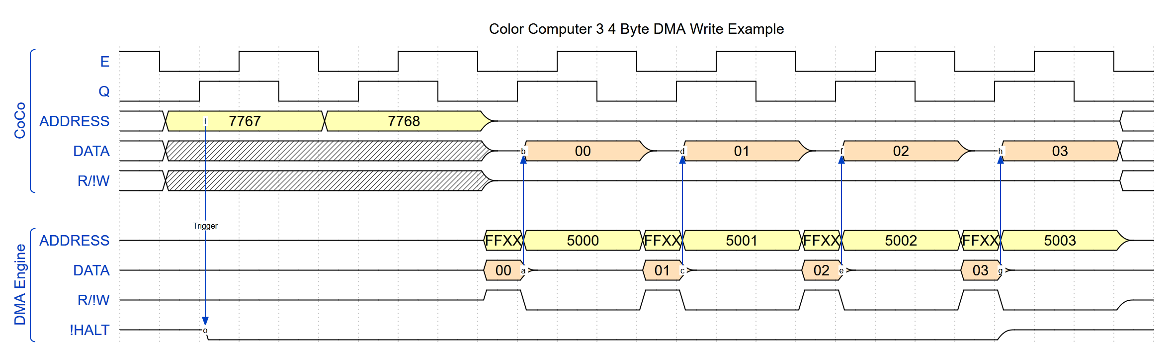
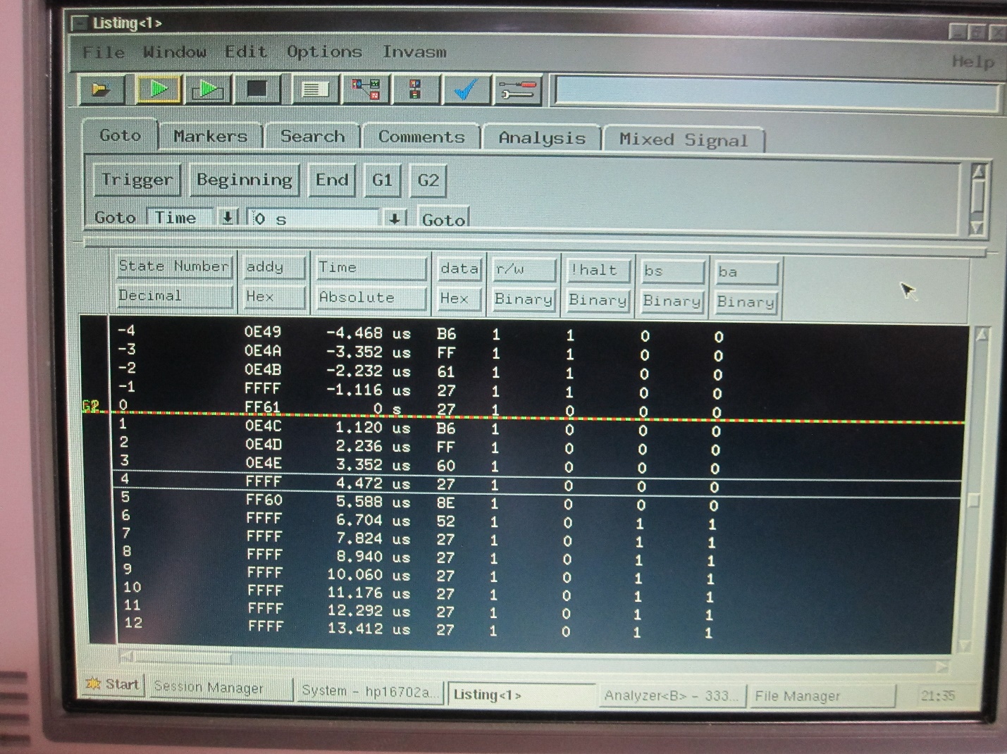
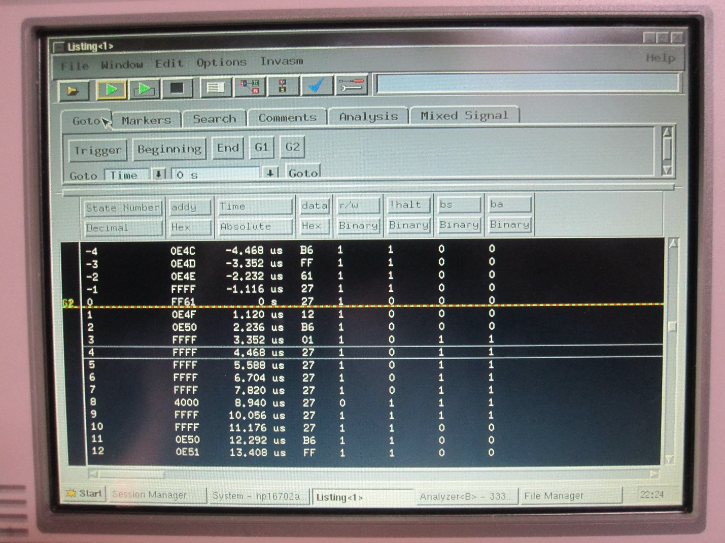
Astute readers have already started wondering: Why is $ffxx placed on the address bus at the beginning of the cycle? Why can’t the desired memory address be placed on the address bus for the entire cycle? To answer that, let’s look at all the items that can place values on the data bus. On the CoCo3, the bus transceiver, the two (2) Peripheral Interface Adapters (PIA), the cartridge port, and the GIME can output data on the bus. Let’s further focus on the first quarter of the CPU cycle, when our DMA engine has placed data on the bus and a read operation has been requested. We already know the 74LS245 bus transceiver is pulling data from the bus, not writing to it. The PIAs specifically gate their reads with the E clock and tri-state the data bus during the low half of the E clock. That leaves the GIME as a possibility.

Interestingly, the data path from the CPU to RAM and the data path from RAM to the CPU (or our DMA Engine) differ, which may surprise some. During write cycles, there are two bus buffers (74LS244) that shepherd data from the data bus into one (1) of the two (2) memory banks (the odd memory locations are in one bank, while the even ones are in another). But, all RAM read accesses pass through the GIME enroute to the CPU. Page 36 stipulates the GIME controls “granting access to the processor during the high time of E (CPU portion)”, which suggests the GIME acts like the PIAs. However, experimentation suggests this is slightly incorrect (or at least somewhat vague).

Since all RAM read accesses travel through the GIME data pins to the CPU, the GIME is allowed to place data on the data bus during any RAM read access. When the Color Computer 3 is configured for an all-RAM memory map, only read accesses to $ff00-$ff7f (I/O region) or $fff0-$ffff (CPU vectors) would be serviced elsewhere. The former would be handled by the PIAs and the cartridge port peripherals, while the latter always reads from onboard ROM. Normally, we would expect the data pins to be inactive during the low portion of the E clock cycle, when the CPU is not accessing the bus. However, possibly due to the need to reduce logic complexity, the GIME tri-states its data bus anytime a write is requested or the above address blocks are accessed, regardless of the state of the E clock cycle. Thus, to ensure the GIME stays off the data bus during the read portion of our DMA write activity, we select an address in one of these areas. We did not experimentally test, but we assume that if a memory map with ROM is selected, all ROM memory locations will also force the GIME to tri-state its data pins (the DMA engine has to select a suitable address given the most restrictive set of requirements/memory map).

As a further note, there is one other portion of the memory map that forces the GIME off the bus during a read cycle. The data sheet for the MC6883 Synchronous Address Multiplexer (SAM), of which the GIME partially emulates, denotes locations $ffe0-$ffef as “Reserved for future MPU enhancements. Do Not Use!” (emphasis in original document). To validate this information, a special version of the DMA Engine was created that allowed the “read address” value to be manipulated by the CoCo3 and all 65536 address values were tested.

We must perform more testing to ensure correct operation across various CoCo3 variations. As well, though we have tested with both MC6809E and HD63C09E CPUs, using stock memory, DRAM-based memory expansions, and SRAM-based memory expansions; various Dynamic Address Translation (DAT) logic options like those found in the Boomerang E2 and Triad+ have yet to be assessed. Initial results, though, look promising, and we are eager for others to replicate Darren’s and my findings.

I would like to take this opportunity to once again thank Darren Atkinson for discovering this solution. Though we both contributed to the final implementation, I can honestly say I would not have considered this path had he not done the initial investigation. As well, I appreciate that, unlike years ago when electronic testing equipment and design tools and services were completely out of the hobbyist’ reach, items like surplus test equipment and PCB CAD software and manufacturing services allow easy investigation into ideas like these.

Now, since we have conquered all of the Color Computer variants, can we do anything else with this DMA idea?

CoCo DMA: Missing Without a Trace

Radio Shack’s introduction of the Color Computer 3 introduced extensive changes to the Color Computer design. Gone were the 6847 VDG and 6883 SAM, functionally replaced and enhanced with the TCC1014 Advanced Color Video Chip (ACVC) which most folks reference as the GIME. Other additions included an additional 64kB of RAM with an option to upgrade all the way to 512kB, support for an additional joystick fire button, and composite and RGB video output options. Almost every addition brought new capabilities or an expansion of capabilities to the Color Computer…

Figure 1: 74LS245 Pinout

Interestingly, for a machine design that I understand focused on parts and cost reduction within TANDY, 1 part was added to the CPU’s data path along the memory bus, an addition that renders our previous work unusable, an addition that breaks the very idea of sharing the bus: the 74LS245 octal bus transceiver. Ironically, the ‘245 transceiver was designed to allow bus sharing. As the name suggests, it contains 8 logic elements, each able to pass one signal from the ‘A’ pin to the ‘B’ pin or vice versa, depending on the state of the “direction” pin. More importantly, when an “enable” pin is de-activated, the logic element effectively “removes” the signal from the pin on the IC. In the industry, the pin is said to be in high impedance mode or “Hi-Z” mode. Such pins are commonly called “tri-state” pins, as they can either output 0, 1, or Hi-Z. The mechanics vary, but the term implies the logic element effectively places such a large resistance in between the signal and the pin that the rest of the circuit can essential ignore or will have no awareness of the signal. The 8 elements, Hi-Z operation, and direction function fit the demands of an 8-bit CPU bidirectional data bus perfectly. We can’t blame the IC itself for this issue, so why does the inclusion of this IC in the Color Computer 3 design render bus sharing unusable?

Let’s peruse the CoCo3 schematic, located on page 103 (or 127 for PAL) of the TANDY Color Computer 3 Service Manual. A snippet is included below in Figure 2. The 74LS245 connects directly to the MC6809E CPU data bus, with the DIR line connected to the CPU R/W line. During normal operation, the CPU drives the ‘B’ lines during a write action, and the ‘245 reads those lines and drives the ‘A’ lines with the same value. On a read activity, the ‘245 reads the data bus ‘A’ lines and drives the ‘B’ lines with that value, which the CPU then reads on its data pins and processes.

Figure 2: CoCo3 CPU Data Bus Schematic

So far, so good. And, all works fine when we perform a DMA-based read action. After halting the CPU, The DMA engine places an address on the bus, and raises the R/W line to read data from memory, just like the CPU. Doing its part, the ‘245 transceiver pulls the data from the ‘A’ pins and places it on the ‘B’ pins, which are connected to the CPU. It’s a nice gesture, though unneeded, since the CPU isn’t running.

Writing, though, is where the issues arrive. Let’s run through the scenario. After halting the CPU, the DMA engine places an address on the address bus, places some data on the data bus, and pulls the R/W line low to signal a memory write. The ‘245, assuming the CPU is trying to write some data to memory, grabs the values on the ‘B’ pins and places the results on the ‘A’ pins, which are connected directly to the shared data bus. The first problem: The CPU is halted, so it is not outputting any data on the CPU data pins. The ‘245 is effectively pulling residual charge from the tri-stated CPU data bus, cleaning it up and driving the data bus. The second problem: Someone else is already driving the bus: the DMA engine. At the very least, the data bus represents an interdeterminate composite of the expected value from the DMA engine and the unknown value from the CPU data pins. More importantly (and more concerning), one output might be attempting to drive a data line low while the other tries to drive it high. In some sense, this is like connecting a battery’s positive post to its negative post. While the amperage involved is much lower, it’s no less damaging to the ICs.

Focus attention on pin 19 of the 74LS245, the “enable” pin, labeled “G”. (I have not yet been able to determine why “G” was used, maybe “gate”. Other versions of the IC use OE, which means “output enable”). Regardless of the name, the bar over the name indicates that it is “active low”. A logic zero (0) on the pin will enable the function. Ground the pin, and the data passes from A to B or B to A. Connect the pin to a “one” (1) signal and all transceiver channels switch into Hi-Z mode. Notice in Figure 2 that the enable line is connected to a symbol that just ends. That symbol is called “chassis ground”, representing a wire connected to a large sheet of metal (the “chassis” of old electronic equipment was made of metal). I won’t go into the specifics of various grounding options (signal ground, earth ground, and chassis ground), but we can all agree this pin is permanently tied to zero (0). Thus, the transceiver is permanently enabled. Good for the CPU, bad for DMA.

On previous Color Computer designs, the 74LS245 was not even included. I don’t know exactly why the functionality was added to the CoCo3, but we can theorize. While dedicated bus transceivers like the ‘245 clean up marginal signals, it’s highly doubtful that signals originating from the MC6809E showed any integrity loss. Bus transceivers like the 74LS245 can also act as “buffers”, protecting (in this case) the CPU from dangerous voltages or skipes on the data bus. Again, this seems dubious, since dangerous voltages on the address bus or other control lines could just as easily damage the CPU, and no buffers are placed on those lines. However, bus transceivers are also used to increase the “drive” capability of a signal. Think of the bus transceiver like an 8 channel amplifier. Each IC connected to the bus uses a bit of power, which must be supplied by the IC driving the bus. ICs thus often specify their drive characteristics in terms of Transistor to Transistor Logic (TTL) “load”, a current requirement of 1.6 milliampere (mA). A standard TTL IC input comprises one (1) TTL load, and a TTL output can typically drive ten (10) TTL loads (16mA). In electronics, this is called the “fanout” rating. Most ICs provide their fanout capability, and the MC6809E specifies a fanout capability of 4 LSTTL loads. A LSTTL (Low Power Schottky TTL), as the name suggests, requires less power than standard TTL. As such, an LSTTL load is equivalent to ¼ TTL load, or 0.4mA. Even if we simplify and consider everything on the CoCo3 data bus as requiring only 1 LSTTL load (0.4mA) each, the CoCo3 attaches 6 items besides the cartridge port and CPU to the databus, which exceeds the 4 LSTTL limit. For comparison, the CoCo1 attaches 5 items, again not including the CPU and the cartridge port. While the MC6809 can probably drive more than 4 LSTTL loads, and CMOS devices like the GIME probably consume less than 1 LSTTL of load, the ‘245 was most likely placed into the design to address this load issue. Now, some will ask, “But, what about the need to boost the drive on the address lines”? It turns out that the address lines are not connected to as many devices (excepting the cartridge port, most address lines only connect to GIME and the ROM, with A0,A1, and A5 signals connecting to 2 more devices).

We’ve determined the bus transceiver is designed to allow bus sharing, and our theory suggests it was a useful addition to the CoCo3 design. So, how should we proceed? As the title of this article suggests, the problem lies in a missing wire in the schematic. Such lines, called printed circuit board (PCB) traces or just traces, connect all of the IC pins in the CoCo3 design. As noted previously, we need one connected to the “enable” pin of the bus transceiver, one that will be zero (0) when the transceiver should be working, and one (1) when the transceiver should be turned off.

Figure 3: MPU States

It turns out that the MC6809E CPU “BA” (Bus Available) line appears to offer the correct operation and polarity. When zero (0), the CPU is utilizing the bus, and while one (1), the bus is “available” for others. Tying the “enable” line to the CPU BA line should allow all existing functionality to continue while enabling CoCo3 DMA operation. That’s the good news. The bad news: adding this trace in some fashion requires hardware modification. Take heart, though, there are a few different ways to proceed.

For reference, let’s look at an NTSC CoCo3 PCB in Figure 4, showing the 74LS245 bus transceiver. You will notice the transceiver sits in between the CPU and the cartridge port (the PAL PCB is slightly different):

Figure 4: CoCo3 PCB

The “enable” pin on the 74LS245 has been denoted with the red arrow, as has the BA pin on the MC6809E (this particular CoCo3 has had the CPU removed and a socket installed).

NOTE: While testing suggests this modification will not adversely affect any current CoCo3 usage, more testing is needed to conclusively prove the point. The below instructions are designed for those who want to modify and confirm operation. Make these modifications at your own risk.

Option 1:

This option requires the least amount of work, but also looks the least pleasing. Simply snip the 74LS245 pin 19 at the spot where it goes into the PCB, bend it up off the PCB, and solder a small wire from it to pin 6 of the CPU. To return to stock, simply remove the wire, bend the pin down, and resolder to the stub in the PCB. Alternatively, desolder and replace the 74LS245.

Option 2:

This option looks neater, but does require cutting a trace.

For this option, remove the PCB from the case, remove the little retaining clips on the shield under the board, and locate pin 19 of the 74LS245. Cut the trace going to that pin, and then solder a wire from pin 19 to pin 6 of the CPU on the bottom of the PCB. To return to stock, unsolder the wire and create a small solder bridge over the cut trace.

Option 3:

This option requires the most work, but it is easiest to convert back to stock.

Figure 5: DMAEnabler PCB

Desolder and socket the 74LS245. Build and populate the DMEnabler PCB shown below, installing the ‘245 into the adapter PCB and then installing the adapter into the CoCo3. Attach a test grabber lead to the BA pin on the adapter PCB and clip the test lead to pin 6 of the CPU. (Enterprising PCB designers could also create a dual-header PCB that fits in both the CPU and the 74LS245 sockets, removing the need for the test lead)

With one of these alterations, normal CoCo3 operation should continue as before, and DMA functionality will be enabled. As teased in last week’s article, with this modification in place, our test application now transfers data from the CoCo3 to external RAM and back:

Figure 6: CoCo3 Transfer to External RAM

While running in FAST mode (poke &hffd9,0), we can see the double read of $ff67/68 trigger the DMA transfer, which then pulls data from $4000-$4003 at ~2MBps.

Figure 7: External RAM transfer to CoCo3

Going the other way, the two cycle $ff67/68 read triggers the engine to push our data to $5000-$5003, again at ~2MBps.

Given that the addition of a single PCB trace into the CoCo3 circuit board would have added no cost and that the inclusion of that trace appears to maintain full compatibility with earlier CoCo systems while also fully enable bus sharing, one can only assume TANDY did not foresee DMA or other bus sharing activities being needed on the cartridge bus or they did not care to support such functions. Alas, requiring a hardware modification to support CoCo3 bus sharing severely limits adoption of this technique. At this point, folks socketing their CPU to upgrade to the Hitachi 63C09 CPU could also start socketing the 74LS245 or otherwise asking this modification be performed, but the majority of CoCo3 units remain unable to utilize this DMA technique.

Still, one cannot help but wonder… What if there were a way to coax an unmodified CoCo3 into sharing the bus? 🙂

CoCo DMA: Invisible RAM

Now that we’ve learned a bit about how the 6809E wants to be treated during a direct memory access (DMA) request, we can put all we’ve learned into action. But, before we launch into the details, let’s address some questions that arose during previous article discussions:

Some asked why the logic doesn’t just watch for M6809E signals BA and BS to both equal 1 (this condition indicates that the CPU is halted), commencing DMA actions at that point. This is my fault. As I started the project effort, I didn’t make it clear that I am trying to determine what DMA capabilities exist at the external side of the TANDY Color Computer expansion port (game cartridge port). I did comment about the expansion port initially, but I should have called that out in more detail. It’s worthwhile to also answer how one enables DMA when inside the computer, but that effort requires modifying the internals of the machine (at least plugging and unplugging ICs, which might not be socketed), and thus trades design complexity for end user complexity. The lowest entry point for DMA exploration (as with most things) is the expansion port, so I’ve concentrated my efforts there. But, for the record, we now know that an internal DMA engine need only pull HALT low, watch for BA=BS=1, and then transfer data as desired.

Others asked if halting the CPU and performing data transfers can really be called “DMA”. Instead of just answering the question by articulating the literal definition of DMA, I believe the question speaks more about how the term “DMA” has evolved over the years. In the beginning, DMA actions made no promises about CPU activity. The act of offloading memory access from the CPU and the act of running the CPU while that alternative access occurred were completely different efforts. In fact, Motorola manufactured and sold a DMA controller IC (the 6844 DMAC) that performed DMA actions by stopping the CPU (in various ways). That said, in today’s IBM PC-based world, where the memory bus, the peripheral bus, and the CPU bus are all separated and tied together with “bridge” ICs, it’s expected that a DMA action will not impact CPU operations. That’s the question being asked. I still believe the answer is “yes”, not only because of the literal definition but also that period-correct implementations would have stopped the CPU. But, I will agree that performing data transfers while not impacting CPU performance would be ideal. The conversation did bring up some neat ideas on how one might share the memory bus, not stop the CPU and perform DMA activities, which we can consider in later installments.

Concerning our primary objective, we now know how to safely stop the CPU and gain control of the bus, and we also know how to manipulate the bus to transfer data from one place to another. But, transferring a single piece of data is boring, so let’s add some more value. On the Color Computer 1 and 2, a fully expanded machine would include 64kB of RAM. Expanding RAM beyond 64kB typically takes 1 of 2 paths:

  • Internal RAM expansion. While CoCo systems were being manufactured, some vendors offered internal memory expansion options that “paged” RAM in 32kB banks. The RAM was easy to access, but the granularity was poor (if you needed 1 byte from another bank, you had to swap out 32kB of code and/or data to access it). Internal expansion solutions also had to contend with motherboard layout differences and lack of socketed ICs.
  • External RAM expansion using the cartridge port. Since the entire address and data bus resides on the expansion port, we can place additional on the bus there. However, due to technical reasons, only 32kB of internal memory can be protected from external memory writes, and I believe external memory cannot be seen by the video subsystem. The currently produced MOOH expansion memory and SD card interface by Tormod Volden represents this category.

There may be value in supporting a third option: DMA memory expansion. Place a large amount of memory external to the machine and enable DMA actions to swap that external memory with the data inside the machine.

Pros:

  • 1 byte granularity. If you need to map in 1 data value, DMA expansion can support that. No 16kB or 32kB banking granularity.
  • No restrictions on memory location. Map in new data anywhere internal RAM exists.
  • No restrictions for video. Map in new data anywhere and the MC6847 VDG can see it.

Cons

  • Slower than banked memory. Each mapped byte takes ~1uS to map.
  • Still limited by internal RAM size. If the CoCo has 4kB of RAM, one can only map in 4kB of data at a time.

Still, in spite of the potential drawbacks, we should implement the idea, if only to use as a stepping stone to more expansive capabilities.

We’ll implement this invisible memory idea by adding some IO registers to our test logic:

  • 3 bytes to hold the memory location in external memory we wish to transfer to/from
  • 2 bytes to hold the memory location in internal memory we wish to transfer from/to
  • 2 bytes to hold the length of memory to transfer
  • 1 byte to configure what type of transfer we want (and some other flags), like:
    • Transfer from internal memory to external?
    • Transfer from external memory to internal?
    • Use a constant address for internal memory (don’t increment internal address after each transfer)?
    • Use a constant address for external memory (don’t increment external address after each transfer)?
    • Enable DMA transfers?

As presented during the last discussion, let’s use the 2 byte “length” parameter as our trigger to start a DMA transfer. This allows the programmer to make most efficient use of code, by leveraging the 16 bit length register as both information sharing and process initiation.

Let’s get into the Verilog code now:

always @(negedge e_cpu or negedge _reset_cpu)
begin
   if(!_reset_cpu)
   begin
      flag_write <= 0;
      flag_mem_hold <= 0;
      flag_sys_hold <= 0;
      flag_active <= 0;
   end
   else if(ce_ctrl & !r_w_cpu)
   begin
      flag_write <= data_cpu[0];
      flag_mem_hold <= data_cpu[5];
      flag_sys_hold <= data_cpu[6];
      flag_active <= data_cpu[7];
   end     
end

  • flag_write = Are we doing a read from internal memory or a write to internal memory?
  • flag_mem_hold = Do not increment the external memory address after every transfer
  • flag_sys_hold = Do not increment the internal memory address after every transfer
  • flag_active = Enable DMA engine

This code just sets the operational flags from the various data bits, or resets them during a reset activity.

always @(posedge e_cpu or negedge _reset_cpu)
begin
   if(!_reset_cpu)
      begin
         flag_halt <= 0;
         flag_knock <= 0;
         flag_run <= 0;
      end
   else if(!flag_dma & ce_knock)
      begin
         flag_halt <= 1;
         flag_knock <= 1;
      end
   else if(!flag_dma & ce_knock2 & flag_knock)
      begin
         flag_knock <= 0;
         flag_run <= 1;
      end
   else if(!flag_dma & !ce_knock2 && flag_knock)
      begin
         flag_knock <= 0;
         flag_halt <= 0;
      end
   else if(flag_dma && (!len))
      begin
         flag_halt <= 0;
         flag_knock <= 0;
         flag_run <= 0;
      end
end

  • flag_knock = access to $ff67
  • flag_run = access to $ff68 after an immediately preceding access to $ff67

This represents a finite state machine with 3 states (IDLE, KNOCK, RUN). I will later optimize this to use a 2 bit “state” value instead of 3 binary bits. Still, I think you can see the sequence. On reset, reset the flags. If $ff67, set flag_knock. If we next see $ff68 (ce_knock), set run flag. The additional check for flag_dma is simply to prevent retriggering a DMA activity while performing a DMA activity that accesses $ff67:68 😊.

always @(negedge e_cpu)
begin
   flag_dma <= flag_active & flag_run;
end

We quantize DMA actions to begin and end on the falling edge of E, and DMA can only occur if the criteria is met and the DMA engine is enabled.

always @(*)
begin
   if(e_cpu & r_w_cpu & ce_addre)
      data_cpu_out = address_mem_out[23:16];
   else if(e_cpu & r_w_cpu & ce_addrh)
      data_cpu_out = address_mem_out[15:8];
   else if(e_cpu & r_w_cpu & ce_addrl)
      data_cpu_out = address_mem_out[7:0];
   else if(e_cpu & r_w_cpu & ce_addrh_sys)
      data_cpu_out = address_sys[15:8];
   else if(e_cpu & r_w_cpu & ce_addrl_sys)
      data_cpu_out = address_sys[7:0];
   else if(e_cpu & r_w_cpu & ce_lenh)
      data_cpu_out = len[15:8];
   else if(e_cpu & r_w_cpu & ce_lenl)
      data_cpu_out = len[7:0];
   else if(flag_dma & !r_w_cpu)
      data_cpu_out = data_mem;
   else
      data_cpu_out = 8'bz;
end

This code looks complicated, but it’s just allowing the developer to read various values. The only condition of interest is the one where flag_dma is active and R/W is 0 (a write to internal memory. In this case, we want to bridge the external memory data bus to the internal memory databus.

always @(*)
begin
   if(!flag_write & flag_dma)
      data_mem_out = data_cpu;
   else
      data_mem_out = 8'bz;
end

Conversely, if we are transferring data from internal memory to external, bridge the CoCo data bus to the external memory data bus.

always @(negedge e_cpu or negedge _reset_cpu)
begin
   if(!_reset_cpu)
      address_mem_out <= 0;
   else if(ce_addre & !r_w_cpu)
      address_mem_out[23:16] <= data_cpu;
   else if(ce_addrh & !r_w_cpu)
      address_mem_out[15:8] <= data_cpu;
   else if(ce_addrl & !r_w_cpu)
      address_mem_out[7:0] <= data_cpu;
   else if(flag_dma & !flag_mem_hold)
      address_mem_out <= address_mem_out + 1;
end

Again, the Verilog looks complicated but is not. We’re simply storing the various pieces of the starting memory address via writes from the CoCo, in 8 bit chunks. During a DMA activity without the address being held, we increment during each falling edge of E.

always @(negedge e_cpu or negedge _reset_cpu)
begin
   if(!_reset_cpu)
      address_sys <= 0;
   else if(ce_addrh_sys & !r_w_cpu)
      address_sys[15:8] <= data_cpu;
   else if(ce_addrl_sys & !r_w_cpu)
      address_sys[7:0] <= data_cpu;
   else if(flag_dma & !flag_sys_hold)
      address_sys <= address_sys + 1;
end

Same story here. We store the internal starting memory address in registers in 8 bit chunks, and we increment the counter by 1 during each cycle if the internal memory address is not being locked into position.

always @(negedge e_cpu or negedge _reset_cpu)
begin
   if(!_reset_cpu)
      len <= 0;
   else if(ce_lenh & !r_w_cpu)
      len[15:8] <= data_cpu;
   else if(ce_lenl & !r_w_cpu)
      len[7:0] <= data_cpu;
   else if(flag_run)
      len <= len - 1;
end

Finally, perform the same action for the length, storing in 8 bit chunks and incrementing while the DMA activity is occurring.

always @(*)
begin
   if(flag_dma)
      begin
         address_cpu_out = address_sys;
         r_w_cpu_out = !flag_write;
      end
   else
      begin
         address_cpu_out = 16'bz;
         r_w_cpu_out = 'bz;
      end
end

Normally, we don’t mess with the address bus, preferring to read it for information. But, during a DMA cycle, we need to place an address on the CoCo bus.

assign _halt = (flag_active & flag_halt ? 0 : 'bz);
assign _ce_ram =!flag_dma;
assign _we_mem =!(flag_dma & !flag_write);

One would think we could use flag_run to configure HALT, but flag_run only goes active after both trigger accesses have happened. Thus, using flag_halt lets us start the HALT condition after the first trigger (access to $ff67) if the DMA engine is active. External memory is selected only during DMA cycles, while the !WE signal to external memory is only enabled if we are reading from internal memory (this signal is overqualified, in that the external memory won’t be active unless flag_dma is active, which means this signal could be simplified to assign _we_mem = flag_write;

After compiling and downloading the firmware into our test cartridge (which contains 512kB of static RAM), let’s see what we can do. We’ll enable the DMA engine (128 => $ff69), set the external address to $000000, internal address to $4000, and length to $0004:

I’d like to interrupt for a second and express appreciation to David Wood (jbevren on IRC and Discord) for pointing me to the VNC server capabilities on my HP logic analyzer. Starting VNC allows me to capture better screenshots and remotely control the logic analyzer.

In this case, we performed a read from $ff67:68, since the program was written primarily in BASIC with a small EXEC to perform LDD $ff67:rts. We can see the $ff67:68 reads, the HALT line going low after the $ff67 access, the wait for $ff68 access, and then 4 reads from internal memory. Before issuing the DMA transfer, I populated $4000-$400a with the ascending values 0-10, and we see them pulled across the data bus in the trace above.

Now, let’s got the other way, transferring those external values back into internal memory at $5000 by turning the DMA engine on, switching transfer direction (129 => $ff69), setting the external address to $000000, setting the internal address to $5000, and keeping the length at $0004:

Again, we see the trigger condition $ff67:68, the HALT condition, and the transfer of our 4 data values from external memory to internal locations, and we see the address incrementing with each transfer. Additional tests show “pinning” an address works as well, which can be useful in the following situations:

  • setting memory to a constant value at 1byte/us by pinning the source address at a location that contains that value
  • Dumping data to the Orchestra 90 or other CoCoSDC at 1MB/s (Yes, the DMA action works even if both the DMA device and the peripheral are external to the CoCo!)

This invisible memory implementation nicely illustrates the DMA capability available on the TANDY Color Computer 1 and 2. Perhaps this knowledge triggers a fellow enthusiast to develop software that will play to the advantages of this memory expansion option. To that end, all resources associated with this effort have been placed under the Creative Commons Share-Alike 4.0 license and uploaded to a GitHub project repository:

https://github.com/go4retro/PhantomRAM/

If interest warrants, PhantomRAM can be turned into a technology solution, though that is outside the scope of this research effort.

Next time, we turn our attention to the 3rd system in the Color Computer lineup and the challenges it poses concerning DMA functionality. Until next time, I present the following two screen shots (hint: check the timestamps 😊)

CoCo DMA: “Fighting on the bus”

Picking up from last time, we were able to successfully place a byte into the internal CoCo memory from the cartridge port without the use of the CPU by utilizing a direct memory transfer procedure. However, after the transfer, BASIC programs would stop with errors at times, machine language programs would simply lock up, and the IO registers of the cartridge device would be corrupted. Clearly, our initial implementation has issues. Since education and understanding drive this effort, we need to dig deeper into the actual bus activity. For that, we must turn to the digital logic designer’s tool of choice: the logic analyzer

For anyone who has even a passing interest in digital circuitry, I (and so many others) strongly recommend obtaining a 10-20MHz dual channel oscilloscope. A multimeter may be the first tool purchased, but an economical dual channel scope should be next on the list. That said, while oscilloscopes are great to see transients and strange signals (like NTSC or audio), they don’t handle digital logic investigation as well. Enter the logic analyzer. Instead of trying to replicate the shape of a signal like a scope, the LA simply detects whether a signal is 0 or 1 (typically using TTL voltage levels as a reference, where 0 = 0-0.8V, and 1= 2.1V-5V). It performs this limited action across many channels, as opposed to the 2 or 4 of a scope. After a scope, I strongly recommend obtaining a small 8-channel USB-based analyzer. They are inexpensive, easy to use, and 8 channels supports simple parallel testing and a plethora of serial protocol testing (RS232, SPI, I2C, etc.). That said, debugging a single board computer or large interface card can take a long time with 8 (or even 16 or 34) analyzer channels. Thus, I also keep a larger professional grade logic analyzer (it used to be the only option, before the USB analyzer options came on the market). Found on eBay from test equipment manufacturers like Tektronix and HP/Agilent/Keysight at reasonable pricing, these units support dozens and sometimes hundreds of analysis channels at frequencies far beyond what the 1980’s computer enthusiast will regularly see.

HP/Agilent/Keysight 16702A Logic Analysis System
Picture 1 of 1
3M 40 pin Test Clip

I’ve recently upgraded my bench analyzer from a 1980’s era HP 1650b (great unit, cheap to buy and own, now passed onto a fellow hardware designer to continue its usefulness) to a 2000’s era HP modular system (HP 16702a). This project gives me my first opportunity to learn how this unit works. I first connect the individual analyzer channels to the various 6809E signals using a 40-pin 3M Test Clip. I highly recommend adding this to your toolbox for signal inspection (the units are expensive if purchased new, but they never wear out, and eBay has more reasonable pricing), as they simplify moving the signal investigation to a new IC or new system. Since we want to investigate all of the bus activity, I place address lines 0-15 under test, as well as data lines 0-7, R/W (read/write), HALT, and the clock signals (E and Q). As we want to know what happens after the access of $ff61, we set a trigger on access to that memory location.

To more accurately pinpoint the issue, we’ll use a hastily (and terribly, I’ll add) written 6809 assembly application to exercise the test device and which exhibits the crashing behavior. A snippet is included below:

lda LOC* grab initial data at $4000
jsr CONVERT * convert binary to hexadecimal and return in D
std SCREEN * store at $0400
lda DMA * execute the DMA action ($ff61)
lda DATA * grab data at $ff60 (the external IO data location)
jsr CONVERT * convert binary to hexadecimal and return in D
std SCREEN+2 * store at $0402
lda LOC * grab data at $4000 (the internal IO data location)
jsr CONVERT * convert binary to hexadecimal and return in D
std SCREEN+4 * store at $0404

Since the application originates at $0e00, the lda DATA instruction after our $ff61 access resides at $0e4c. When we run the test program, the logic analyzer triggers and the program crashes. But, the evidence surfaces. On the logic analyzer, we see the following:

Address Data R/W HALT Notes
0e49 b611
0e4a ff11
0e4b6111
ffff2711Dead Cycle
ff612710Nothing at $ff61, but bus rests at $27
40002d01 Our data write ($2d = 45)
We sample on falling E, so HALT=1
0e4d ff11 Why did we jump to $0e4d?

Folks probably start to see what is going on, but it pays to be sure. The Verilog is modified to not activate the address bus or R/W line, hold HALT low forever, and the test is repeated. Here is the result:

Infinite HALT condition

The problem begins to show itself. Even though the device has pulled HALT low before the end of the instruction execution, the CPU reads and executes one more instruction before releasing the bus. We can tell because of the state of the BS and BA lines. The 6809 datasheet notes that BS=BA=1 signifies a HALT condition in the CPU. Further attempts to pull HALT low earlier in the $ff61 read cycle make no difference.

Darren Atkinson (of CoCoSDC design fame) emailed after hearing about the project effort, asking about HALT line triggering. I initially misread his email as inquiring whether I had pulled HALT low early enough in the instruction cycle. But, Darren responded again and pointed to a key portion of the datasheet I had misinterpreted:

6809E Datasheet HALT Condition Specifics

Hint: It’s the text at the top of the page. I noticed the “2nd to Last Cycle of Current Instruction” notation, but interpreted it to be illustrating to the reader that activating the HALT line before the last cycle of an instruction would not cause an immediate reaction. From my days working with the 6502, I knew that 8-bit processors are not designed to maintain an intermediate instruction state for any length of time. The CPU assumes that once an instruction is started, it must complete before anything else will be processed. While this doesn’t seem to be a concern for the HALT condition (just simply stop the processor, wait for HALT to become inactive, and continue on), it makes sense that HALT would use the same sense logic and internal handling logic as interrupts, and stopping the CPU in mid-instruction to handle an interrupt would require saving an intermediate instruction state. Thus, for that reason, the simpler 8-bit CPUs just don’t do that. Once an instruction opcode is fetched, the CPU will fully execute the current instruction before handling any event. If the datasheet showed the HALT line going low on the last cycle, it could imply that execution would stop at the end of the current instruction cycle. Thus, I thought this text was simply reinforcing the text describing the HALT pin: “A low level on this input pin will cause the MPU to stop running at the end of the present instruction and remain halted indefinitely without loss of data”.

However, my assessment was plain wrong. As Darren pointed out, the “2nd to last instruction” text carries crucial significance. As well, it’s the key to the problem we are experiencing. The Verilog is activating HALT on the last cycle of the current instruction, which is actually too late. The CPU moves ahead to read and process the next instruction, only then latching and acting on the HALT condition. I wish this prerequisite had been noted somewhere in the datasheet, but I checked the 6809E, the 6809, the 63C09E and the 63C09 datasheets online and in my possession and found no mention of the constraint. That said, a Facebook commenter also pointed out this requirement, so perhaps everyone in CoCo land knows this tidbit of information.

Now that we know the issue, how do we solve it? I first added a NOP to the code, thinking that doing so would allow the next real instruction to be read correct (the lda $ff60). However, before testing, I quickly realized that would not work. Since the CPU is still reading an opcode, it would interpret any data on the databus during that cycle as the next opcode, potentially altering the program anyway. I next added Verilog code to wait an arbitrary 8 cycles after HALT activation before accessing memory:

HALT with 8 wait states
  • The read from $ff61 happens, and HALT is activated
  • A NOP is read
  • The next instruction is read (the second cycle of a NOP instruction appears to read and discard the next opcode)
  • Then the CPU is halted (as shown by the BS=BA=1 condition
  • The Verilog waits a few more cycles (shown as $ffff:$27 read cycles)
  • Then the data is transferred to 4000 (in this test, the written value was $27) while HALT is deactivated.
  • The CPU takes a cycle to acknowledge the deactivation
  • The CPU takes another cycle to prepare for startup
  • Then, the $b6 opcode (of lda $ff60 instruction) is read

Success! BASIC test applications begin running to completion with no unexpected errors, and the test machine language application no longer crashes the machine, instead it runs to completion and illustrates that all 256 values can be transferred from outside the machine to internal memory locations.

That said, adding dead cycles to the DMA engine is far from ideal. In fact, after Darren noted that a full register stack-up could take 20+ cycles on a 63C09, I quickly found the dead cycle wait idea untenable. Clearly, we need to find a better way to trigger a DMA transfer. I quickly sketched out a few requirements and some preferences:

  1. The action must pull HALT low prior to the second to last instruction cycle
  2. The condition must not occur over two consecutive opcodes (interrupt could occur in between)
  3. The condition must not require scanning the databus for specific opcode/operand sequences (i.e. watch the databus for $b6,$ff,$61)
    1. Doing so requires constantly activating the SLENB line when installed in an MPI, since the data bus is hidden from MPI slots unless an IO access is made or SLENB is activated. And, SLENB being activated on arbitrary memory locations would cause other problems
    2. There’s no guarantee such a sequence would never occur in any other way.
  4. Ideally, the “trigger” action should be an instruction that would be otherwise needed (so as to not waste any time performing some action JUST to start the transfer)
  5. If a memory address trigger, the address should be constant

I just as quickly decided that CPU instructions that perform 2 memory accesses in a single instruction would ideally suit these constraints. HALT could be triggered to go low on the first memory access, and if the second memory access did not occur 1 or 2 cycles later, the HALT condition would become inactive and the system would not perform the transfer. If the condition was met, the system initiate a transfer after the second memory access. I first gravitated to INC $ff61, which performs a ®ead-(M)odify-(W)rite action (reading the memory location, adding 1 to the value, and writing it back to memory). Since INC $ff61 performs a read cycle, then takes an internal cycle to perform arithmetic (ALU) operations, and finally writes the new value back, the Verilog state engine needed to detect the initial access, wait a cycle, and then detect the second access. That’s not hard to support, but it’s wasteful. Supporting preference #4 proves the larger challenge. Rarely would someone need to increment a value in the DMA engine register set. While I was debating options, fellow enthusiast and Nitros9 developer L. Curtis Boyle suggested LDD, which performs 2 consecutive memory accesses in 2 consecutive cycles. While LDD may not be of great use, STD (store D) would often be used to place a 16 bit value in the registers, as would other 16-bit memory store operations. Since it also simplifies the Verilog, we will utilize it as the DMA transfer start mechanism. In essence:

  • Once the lower IO register is accessed, bring HALT low and set flags
  • In the immediate next cycle:
    • If the next higher IO address is accessed in the next cycle, continue to hold HALT low and prepare for a DMA transfer
    • If not, release the HALT line and do not prepare for a DMA transfer

If the first condition is met but not the second, the CPU will likely notice the HALT condition and stall for 2 cycles after the current instruction, but no harm will arise. To prevent accidental DMA activity while setting register values, we should also add a bit in the eventual control register to enable or disable DMA transfers.

More testing is needed to understand other issues, if any, with assuming a transfer can begin immediately following an LDD/STD type instruction. Since Darren Atkinson already broached the subject of interrupt handling, he performed a test that activated NMI and HALT at the same time, attempting to understand which behavior took precedence. Darren utilized the following circuit and program snippet:

By organizing the stack right above screen memory and driving NMI and HALT low with an SCS access to $ff40, NMI precedence would show as characters on screen (stack values). When executed, no such values appeared, which strongly suggests HALT takes precedence over interrupts.

Now that we have verified the ability to safely transfer data from outside the CoCo to internal memory without disrupting program execution and a way to reliably and atomically trigger such a transfer, we will put all of the pieces together into action. Many thanks to those following along on this journey so far, and a special thanks to Mr. Atkinson for his insights.

CoCo DMA Early Efforts

As referenced in http://www.go4retro.com/2020/02/26/direct-memory-access-possibilities-on-the-tandy-color-computer/, I am attempting to coax some direct memory access functionality from a TANDY Color Computer. I’ll be utilizing a TANDY Color Computer 1 for initial testing, as I feel it most closely matches the Motorola 6809 reference architecture and this year is the 40th anniversary of the machine’s introduction.

As noted in the last article, the !HALT signal is key to enabling DMA functionality (if possible at all) on the 6809. The datasheet stipulates that this line must fall no later than 200nS (for a 1MHz CPU) before the falling edge of the Q clock to ensure correct operation. As well, the signal must rise 200nS prior to the Q clock falling edge of the last DMA cycle. It turns out that, for a ~1MHz system, each of the 4 clock phases exhibited by the two clock signals (E and Q) last 250nS:

  • eq = 250nS
  • eQ = 250nS
  • EQ = 250nS
  • Eq = 250nS

Thus, to ensure our signal becomes active 200+nS before the fall of Q, we can simply enable the signal at the rising edge of E. Coupled with the fact that the CoCo 1 runs a bit slower than 1MHz (.89MHz), we have over 40nS of buffer.

As previously noted, I am utilizing a Complex Programmable Logic Device to simplify the hardware portion of these tests. To make the device perform work, I write the logic in the Verilog Hardware Description Language (HDL). Since I develop in the C programming language, I chose Verilog since it resembles C in some respects (functions, assignment, case statements, etc.). One can also program in VHDL, which is often compared to ADA (its verbosity reminds me of COBOL, actually), but these can spark religious debates. Suffice it to say that Verilog works well for me, and others may find other solutions. Cue the Verilog writing-style comments 🙂

I’ll dispense with the module definition, since it’s pretty standard (it resembles a C function definition), and get right to the important parts:

assign ce_reg = (address_cpu[15:4] == 12'hff6);
assign ce_test = ce_reg & (address_cpu[3:0] == 0);
assign ce_start = ce_reg & (address_cpu[3:0] == 1);

I’ve situated the hardware registers in the CoCo IO range, and moved them out of the way of a floppy drive controller. This allows me to test my hardware with a floppy drive using a simple ‘Y’ cable. We’ll set up a storage register at $ff60 for a value to DMA back to the CoCo, and we’ll use $ff61 to start a transfer.

register #(.WIDTH(8)) reg_test(
q_cpu,
!_reset_cpu,
ce_test & !r_w_cpu,
data_cpu,
data_test
);

This just points to a user developed module defined elsewhere that creates little 74ls574-like devices to hold data, clocked on the falling edge of Q, using data_cpu as the input, and placing the result in data_test.

always @(*)
begin
if(e_cpu & r_w_cpu & ce_test)
data_cpu_out = data_test;
else if(flag_dma)
data_cpu_out = data_test;
else
data_cpu_out = 8'bz;
end

When one has a bunch of assignment options in Verilog, this is an ideal way to compose the logic. Essentially, since I dislike “write-only” registers, the first condition checks if someone is trying to read the value from $ff60 or not. The second condition is our DMA transfer condition, and the third (default) condition places the output lines in a tri-stated configuration. Yes, I could combine the first and second conditions, but I’ll not do that.

always @(posedge e_cpu)
begin
if(ce_start)
flag_halt <= 1;
else
flag_halt <= 0;
end

As discussed earlier, we want !HALT to go low at the rising edge of E, and go high in the same spot when the DMA cycle is concluding. Since we’re only doing a single DMA transfer, this code works fine.

assign _halt = (flag_halt ? 0 : 'bz);

We’ll use our flag to push the !HALT line low or keep it tristated (!HALT is like !IRQ and !FIRQ and !NMI, in that they are all “wired-or” type signals.

always @(negedge e_cpu)
begin
if(flag_halt)
flag_dma <= 1;
else
flag_dma <= 0;
end

While we have to handle the !HALT line essentially in the middle of the cycle prior to the DMA, we can’t start the actual DMA cycle that early. This Verilog allows us to position the DMA cycle at the beginning and ending boundaries of the E cycle, which defines the CPU clock cycle.

always @(*)
begin
if(flag_dma)
begin
address_cpu_out = 16'h4000;
r_w_cpu_out = 0;
end
else
begin
address_cpu_out = 16'bz;
r_w_cpu_out = 'bz;
end
end

If we’re in a DMA cycle, place $4000 on the address bus (arbitrary testing address) and set R/W to 0. Otherwise, tri-state both sets of signals.

All that remains is to compile the Verilog into a suitable JEDEC bit file and download into the Xilinx 95288XL-6 144 pin CPLD 5 volt tolerant CPLD. Yes, it’s overkill for this test (just a few IO would have been plenty), but it’s what was close at hand, and using a large part for initial development allows on to focus on the code rather than the size of the code. This unit has a 6nS latency, which must be added to all signal timings.

On the CoCo1 side, we need to write a small test program. In this case, let’s just place 45 in the CPLD register, issue the DMA cycle, and see if it made it’s way to $4000.

1 poke &hff60, 45: poke &h4000,0
2 ? peek(&hff60);
3 a = peek(&hff61): rem don't care, just need something to hit that address
4 ? peek (&h4000)

After downloading the Verilog firmware, writing the CoCo BASIC program, and executing, we see the following on the logic analyzer:

Figure 1: 6809 DMA Example

We see the !HALT line going low right as the E clock goes high, and then we see the R/W line falling just as the previous cycle end and the next cycle starts. In the midst of the DMA cycle, we see the !HALT line rise, which meets the timing requirements.

The results? Promising. After running the test, location $4000 contains the expected 45, so the write completed successfully. However, all is not right as yet.

  1. After a transfer, the value in $ff60 is corrupted. Not sure why that would be, but I suspect it related to #2
  2. For some test values, BASIC will return an error during the A=peek(&hff61) line and stop the program.

Removing the line that places the test data on the data bus during a DMA cycle eliminates the issue, which means the mere presence of data on the data bus during a DMA cycle is an issue. The next step is to wire up the CPU to a larger logic analyzer, one that can consume all of the address and data lines of the 6809 at one time. The good news is that I have just recently purchased a HP 16702A Logic Analysis System economically (from eBay) and outfitted it with 2 16717A 68-channel 333MHz timing logic analysis cards (134 logic channels in total, though 1 will suffice for this CPU). Now, I just need to learn how to use it (it’s a sight more complex than my older HP 1650B logic analyzer). Off to debug!

Direct Memory Access Possibilities on the TANDY Color Computer

As part of my continuing efforts to understand direct memory access (DMA) capabilities of various 80’s home computer systems, I decided I should figure out what, if any, DMA capabilities are possible on the TANDY Color Computer systems. There are 3 essential models in the lineup, though from a technical perspective, I feel there are 2 main variants: The CoCo1 and 2, which share very similar features and capabilities (mainly, the difference is in some cost reduced circuitry in the 2 and more memory in the later machines) and the CoCo3, which contains a more capable video processor, substantially more memory, and a memory management unit (MMU). Most folks also consider the Dragon Data Dragon machines as part of this lineup, and those are roughly similar to the CoCo1/2 systems (both systems seem to be based on a Motorola reference design. The CP1400 might also qualify, but I don’t have one and know little about the design, so I will consider the 4 above machines inclusively

A pre-requisite for DMA operation is an ability to stop the running CPU in some fashion and a way to access internal memory and/or IO from the cartridge or expansion port. The VIC-20, for example, has no way to stop the running CPU, so DMA is not possible. However, TANDY (and Dragon Data) helpfully provided a pin on the expansion port that will temporarily shut off the internal Motorola M6809E CPU and remove its address and data signals from the system bus (this part is essential, because if the CPU is not running but it still outputs address and data on the system bus, the bus is not available for other users). On the M6809E, that signal is called !HALT and is active low. To “halt” the 6809 CPU, simply bring this line low on the expansion port during a cycle. Of course, nothing is that simple, so here’s some more detail:

Figure 8: HALT behavior

!HALT can be pulled low anytime, but will only take effect if it falls 200nS or more before the falling edge of Q (Q is 1 half of the 4 phase clock system used by the 6809 and typically is high during the middle of the CPU clock “cycle”). This consideration is called tPCS on the timing diagram, and is 200nS for a 1MHz CPU, 140nS for a 1.5MHz, and 100nS for a 2MHz CPU. As well, one can bring !HALT high at a later time, but it again must occur tPCS nS before the fall of the Q clock signal. Still, if one adheres to those rules, the entire address and data bus (on the CoCo1 and 2, anyway) is available at the expansion port for reading from and writing data to the internal memory.

One must crawl, then walk, and then run in these efforts, so the first thought is to figure out the !HALT signalling and attempt to transfer a single value from the expansion port to an internal memory location. Testing would then involve setting the internal memory location to a value other than the one expected, triggering the DMA functionality, and then looking at the internal memory location. If the value has been changed, one can be confident a DMA transfer has occurred. Once that is in place, it can be used as a foundation to expand the functionality to support the transfer of many data values to many locations, and then digress into the various useful DMA use cases (fast floppy emulator, extra memory on demand, feeding audio data to a DAC, etc.). But, it’s a tall order to transfer that first byte, so let’s focus on the task at hand.

Many years ago, I would approach this by grabbing a perfboard and wiring up some 74LS TTL logic ICs on the board to approximate the functionality desired. Of course, it would be wrong, so many hours of rewiring and soldering up new ICs would be involved. Now, though, as much as some retro enthusiasts object, I utilize a suitable Complex Programmable Logic Device (CPLD) attached to a small cartridge PCB to efficiently design the required logic. While soldering and deciding on the correct TTL IC has value, if you’re trying to make something work, those activities can get in the way of the design process. A CPLD allows one to change the design simply by modifying the “software”, downloading it into the IC, and testing. Once the design is working, one can translate back into TTL ICs if desired, or (in many of my recent designs), simply continue to utilize a CPLD. CPLDs are the children of PLDs like the 16v8 PAL used in the 1980’s, and some CPLD variants were available in the era of these machines. These complex devices can replace dozens of ICs in a design, decreasing finished unit costs consderibly and bringing these types of functions well within the grasp of hobbyists to manufacture and enthusiasts to buy. Since I’ve always desired to create economical solutions for these classic machines, the CPLD provides significant value. Still, for the moment, I’m most interested in the design efficiencies, especially since there’s no guarantee anything will work in the end.

RAM Expansion for the C64

RAM expansion was a common topic in the Commodore 64 community in the 1980’s.  Everyone seemed to need or want more RAM:

  • Soon after the unit arrived in stores, Paul Bosacki published a way to upgrade the unit to 512kB
  • Later, he pushed the expansion to 1MB
  • Berkeley Softworks (later GeoWorks), jumped into the fray with the 512kB GeoRAM
  • After the C128 arrived, Commodore got in the act, coming out with the 1700, 1764, and 1750 RAM Expansion Units, providing 128kB, 256kB, and 512kB of RAM, respectively.
  • Lots of people soon determined all 17XX units could be upgraded to 512kB
  • And, then, Andrew Mileski furthered that idea by piggybacking DRAM and pushing the 17XX to 2MB

Over time, RAM expansion options for the C64 have coalesced around two types: REU and GeoRAM.  The REU is much faster, but the GeoRAM is easier to create and use.

Still, both suffer from a serious issue.  Neither one makes RAM immediately available.  Both contain RAM outside the CPU’s direct access.  The Commodore REU can transfer memory from the unit to main system RAM around 1 million bytes/sec, while the GeoRAM has more humble speeds around 125KB/sec.  Sometimes, though, one would like RAM to be instantly available.

Cartridges like EasyFlash and EasyFlash 3 map FLASH ROM directly into the C64 memory map to simplify writing cartridge data.  Along those lines, it should be possible to map RAM directly into the C64 memory map as well, using the impressively capable and mysterious “Ultimax” mode.

The idea:

  • Treat the C64 memory map as 16 slices of memory, each 4KB in size. 
  • Allow the developer to select which portion of external RAM will “reside” in each 4kB slice.
  • If the developer maps a slice of RAM, any read or write access to that RAM will trigger Ultimax mode and place the external RAM onto the system bus during a CPU cycle.

The functionality shares a lot with UltiMem, a product we offer for the VIC-20.  But, the programmer can grow weary of manually configuring and reconfiguring each 4kB slice each time he/she wants to move to a different piece of RAM.  For that, we should take a page from the C128 MMU and create the idea of a “mapping set”.  A mapping set comprises 16 values, one for each slice of main memory.  The C128 supports 4 different mappings, which makes the developer’s job easier.  Set up the mapping and then just use it when needed.

So, let’s add a few more features:

  • Support a “mapping set” of 16 values
  • Support multiple mapping sets, which can be selected by storing a value into a specific register to denote the mapping set “ID”

Finally, though the Commodore REU may be too complicated to implement:

  • Support GeoRAM registers for backwards compatibility

One should be wary of announcing success too early, but initial development shows this functionality is possible.  At this point, the following functionality appears to be working:

  • 512kB of SRAM
  • GeoRAM register support
  • Support for 128 “mapping sets”
  • All memory slices except slice 0 and slide ‘D’ can reside externally

Of course, at this point, once something works, one needs to determine if anyone cares 🙂 

New(ish) Project: VIC-MIDI

VIC-MIDI Prototype
VIC-MIDI Prototype

This project had its start in a late 2009 discussion between Leif Bloomquist, a Canadian Commodore enthusiast and musician, and myself.  Leif had been playing with a hand-built 6850-based VIC-20 MIDI cartridge designed off a 1980’s era Maplin “Electronics” article, and wondered if a production run could be arranged.  I took a look at the design, and noted that the 6850 UART would be hard to source.  I suggested some design changes to bring costs down, and plans were made to refine the design.

To further the design, I wired up a newer UART (16450-based) to a daughtercard that could plug into the 6850 socket on the original board.  That allowed Leif to refine the software, and provide out the redesign.  Once that was done and successful, we discussed a final production version.  Changes included offering a built-in user-flashable ROM function.

That brings us up to late 2012.  I purchased the parts for a completely new prototype board, but could not get it assembled by World of Commodore, so I brought the parts to the show and hired the assembly done.

Well, the assembly resource took longer than expected to finish the construction, but I did receive this same exact board mid-Feburary 2013.  I fixed a few small design issues, only to discover the board expansion port was wired 100% backwards.  Commodore, for reasons known to them only, named the pins on the VIC-20 expansion port in reverse from the industry standard.  Since the prototype PCB pins were named according to the standard, every one would need modification.

I packaged up the board and sent it back to the assembler, but I must have messed up the address, as it did not arrive in a timely fashion.  Since I had shipped it from the Post Office directly, I didn’t get tracking information, and thus had no idea of its location.  After a few weeks, I resigned myself to the loss of the unit, and started gathering parts for a second unit to be shipped via trackable shipment to the assembler.  As it turns out, the assembler and I were both planning to attend the 2013 Midwest Gaming Classic in WI, so I made plans to transfer a new set of parts during the show.

No sooner than the show ended and parts were transferred, the original package showed up at my office, undeliverable.  I quickly saw the addressing issue, created a new trackable label with the correct address, and sent it on its way.  Which brings us to last week, when the unit arrived, after the rewiring effort.

After all of that effort, I could now begin the potentially laborious task of debugging a “paper design”.  I had designed the entire unit on paper, but had not previously proven out any of the elements on a breadboard.  Though the original UART design was working on Leif’s PCB, the new design was marked different, owing to the additional decoding logic needed for the FLASH ROM.  As such, it was almost a completely new design.   I’m not sure if credit is deserved and who deserves it, but the UART and FLASH ROM read access worked out of the box.  Bank selection for the FLASH ROM did not work, but that’s a minor issue.

And, we’re almost to the point of creating a VIC-20 MIDI production design.

New Project: IECSwitch

IECSwitch v0.1
IECSwitch v0.1

I can’t claim a significant amount of creativity, but over the past few years, two folks have dropped off “VIC-Switch”-like devices in hopes that I could reverse engineer them.  THese are devices used back in the day (typically in schools) to share a single disk drive or disk and printer with up to 8 computers. I long ago drew up schematics of the existing designs, but wanted to freshen up the solution instead of just creating a replica.

Well, as it goes, finding time takes time, but I decided to try my hand at a new design, and here is the current result.  It’s not much at present, though I can enable/disable IEC ports, and “hold” the 64 from timing out the bus request.  Yes, that’s an LCD there.  I found a great price on them, and I think that’ll be in the final design.  It’s only marginally cheaper than a 7 segment LED or two, and much more interactive then a few LEDs.

It’s been awhile since I developed firmware, and this gave me a chance to clean the cobwebs off my programming skills.

Coming Soon: SuperOS/9 MMU Kit

SuperPET OS/9 MMU
SuperPET OS/9 MMU

In the “another project that has been long in gestation” category comes a niche offering for those with Commodore SuperPET machines and a desire to run the OS/9 operating system.  OS/9, a multi-tasking, multiuser, realtime OS with UNIX-like qualities, was popular in the 1980’s and ran on machines with the Motorola 6809.  In addition to the small TRS80 Color Computer, the SuperPET includes a 6809, but the standard memory map of the SuperPET does not lend itself to OS/9 operation.  That is where this little board comes in.  Installation does not affect normal SuperPET operation, but extends it with OS/9 compatibility.

The SuperPET, a variant of the Commodore 8032 that included additional boards designed by the University of Waterloo, did not sell well, as far as I can tell, and limited (though not ultra-rare) numbers exist.  Still, for those lucky enough to own one, OS/9 can truly turn the SP9000 (another name for the SuperPET) into the MicroMainFrame (another name for the SuperPET).

The project has been gestating since 2008 in some fashion.  Late that year, TPUG member Golan Klinger asked if I could reproduce the SuperPET MMU board, which TPUG members created in 1985. for a possible club fundraising activity.  I dutifully created a new layout of the design, and awaited next steps.  Around the same time, Mike Naberezny (of 6502.org fame) started discussing the board, and we eventually compared notes.  Over time, it became evident that TPUG was not going to pursue offering the unit for sale, and Mike performed a significant amount of legwork obtaining permission to replicate the software from Radisys (who purchased the OS/9 rights) and permission from TPUG leadership to offer the PCB.  Thus, the majority of credit for this offering goes to Mike, who has a web site devoted to this impressive little board.  I’ll put one in due time, but it won’t provide any more detail than Mike’s.  I should also give a shout out to Steve Gray, who helped with information and PCB scans.

Currently, due to the low volumes, the unit will be available in kit form only for approximately $30.00.  Thus, break out your soldering iron and a weekend of time to add this capability to your SuperPET!