As referenced in https://www.go4retro.com/2020/02/26/direct-memory-access-possibilities-on-the-tandy-color-computer/, I am attempting to coax some direct memory access functionality from a TANDY Color Computer. I’ll be utilizing a TANDY Color Computer 1 for initial testing, as I feel it most closely matches the Motorola 6809 reference architecture and this year is the 40th anniversary of the machine’s introduction.
As noted in the last article, the !HALT signal is key to enabling DMA functionality (if possible at all) on the 6809. The datasheet stipulates that this line must fall no later than 200nS (for a 1MHz CPU) before the falling edge of the Q clock to ensure correct operation. As well, the signal must rise 200nS prior to the Q clock falling edge of the last DMA cycle. It turns out that, for a ~1MHz system, each of the 4 clock phases exhibited by the two clock signals (E and Q) last 250nS:
- eq = 250nS
- eQ = 250nS
- EQ = 250nS
- Eq = 250nS
Thus, to ensure our signal becomes active 200+nS before the fall of Q, we can simply enable the signal at the rising edge of E. Coupled with the fact that the CoCo 1 runs a bit slower than 1MHz (.89MHz), we have over 40nS of buffer.
As previously noted, I am utilizing a Complex Programmable Logic Device to simplify the hardware portion of these tests. To make the device perform work, I write the logic in the Verilog Hardware Description Language (HDL). Since I develop in the C programming language, I chose Verilog since it resembles C in some respects (functions, assignment, case statements, etc.). One can also program in VHDL, which is often compared to ADA (its verbosity reminds me of COBOL, actually), but these can spark religious debates. Suffice it to say that Verilog works well for me, and others may find other solutions. Cue the Verilog writing-style comments 🙂
I’ll dispense with the module definition, since it’s pretty standard (it resembles a C function definition), and get right to the important parts:
assign ce_reg =                        (address_cpu[15:4] == 12'hff6);
 assign ce_test =                       ce_reg & (address_cpu[3:0] == 0);
 assign ce_start =                      ce_reg & (address_cpu[3:0] == 1);
I’ve situated the hardware registers in the CoCo IO range, and moved them out of the way of a floppy drive controller. This allows me to test my hardware with a floppy drive using a simple ‘Y’ cable. We’ll set up a storage register at $ff60 for a value to DMA back to the CoCo, and we’ll use $ff61 to start a transfer.
register #(.WIDTH(8))                   reg_test(
                                                  q_cpu,
                                                  !_reset_cpu,
                                                  ce_test & !r_w_cpu,
                                                  data_cpu,
                                                  data_test
                                                );
This just points to a user developed module defined elsewhere that creates little 74ls574-like devices to hold data, clocked on the falling edge of Q, using data_cpu as the input, and placing the result in data_test.
always @(*)
 begin
    if(e_cpu & r_w_cpu & ce_test)
       data_cpu_out = data_test;
    else if(flag_dma)
       data_cpu_out = data_test;
    else
       data_cpu_out = 8'bz;
 end
When one has a bunch of assignment options in Verilog, this is an ideal way to compose the logic. Essentially, since I dislike “write-only” registers, the first condition checks if someone is trying to read the value from $ff60 or not. The second condition is our DMA transfer condition, and the third (default) condition places the output lines in a tri-stated configuration. Yes, I could combine the first and second conditions, but I’ll not do that.
always @(posedge e_cpu)
 begin
    if(ce_start)
       flag_halt <= 1;
    else
       flag_halt <= 0;
 end
As discussed earlier, we want !HALT to go low at the rising edge of E, and go high in the same spot when the DMA cycle is concluding. Since we’re only doing a single DMA transfer, this code works fine.
assign _halt = (flag_halt ? 0 : 'bz);
We’ll use our flag to push the !HALT line low or keep it tristated (!HALT is like !IRQ and !FIRQ and !NMI, in that they are all “wired-or” type signals.
always @(negedge e_cpu)
 begin
    if(flag_halt)
       flag_dma <= 1;
    else
       flag_dma <= 0;
 end
While we have to handle the !HALT line essentially in the middle of the cycle prior to the DMA, we can’t start the actual DMA cycle that early. This Verilog allows us to position the DMA cycle at the beginning and ending boundaries of the E cycle, which defines the CPU clock cycle.
always @(*)
 begin
    if(flag_dma)
       begin
          address_cpu_out = 16'h4000;
          r_w_cpu_out = 0;
       end
    else
       begin
          address_cpu_out = 16'bz;
          r_w_cpu_out = 'bz;
       end
 end
If we’re in a DMA cycle, place $4000 on the address bus (arbitrary testing address) and set R/W to 0. Otherwise, tri-state both sets of signals.
All that remains is to compile the Verilog into a suitable JEDEC bit file and download into the Xilinx 95288XL-6 144 pin CPLD 5 volt tolerant CPLD. Yes, it’s overkill for this test (just a few IO would have been plenty), but it’s what was close at hand, and using a large part for initial development allows on to focus on the code rather than the size of the code. This unit has a 6nS latency, which must be added to all signal timings.
On the CoCo1 side, we need to write a small test program. In this case, let’s just place 45 in the CPLD register, issue the DMA cycle, and see if it made it’s way to $4000.
1 poke &hff60, 45: poke &h4000,0
2 ? peek(&hff60);
3 a = peek(&hff61): rem don't care, just need something to hit that address
4 ? peek (&h4000)
After downloading the Verilog firmware, writing the CoCo BASIC program, and executing, we see the following on the logic analyzer:
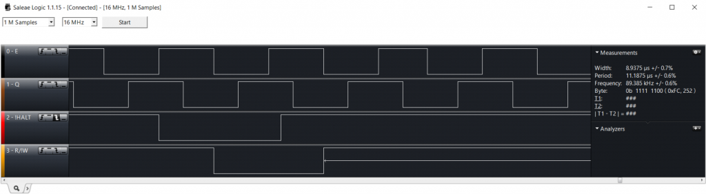
We see the !HALT line going low right as the E clock goes high, and then we see the R/W line falling just as the previous cycle end and the next cycle starts. In the midst of the DMA cycle, we see the !HALT line rise, which meets the timing requirements.
The results? Promising. After running the test, location $4000 contains the expected 45, so the write completed successfully. However, all is not right as yet.
- After a transfer, the value in $ff60 is corrupted. Not sure why that would be, but I suspect it related to #2
- For some test values, BASIC will return an error during the A=peek(&hff61) line and stop the program.
Removing the line that places the test data on the data bus during a DMA cycle eliminates the issue, which means the mere presence of data on the data bus during a DMA cycle is an issue. The next step is to wire up the CPU to a larger logic analyzer, one that can consume all of the address and data lines of the 6809 at one time. The good news is that I have just recently purchased a HP 16702A Logic Analysis System economically (from eBay) and outfitted it with 2 16717A 68-channel 333MHz timing logic analysis cards (134 logic channels in total, though 1 will suffice for this CPU). Now, I just need to learn how to use it (it’s a sight more complex than my older HP 1650B logic analyzer). Off to debug!