Radio Shack’s introduction of the Color Computer 3 introduced extensive changes to the Color Computer design. Gone were the 6847 VDG and 6883 SAM, functionally replaced and enhanced with the TCC1014 Advanced Color Video Chip (ACVC) which most folks reference as the GIME. Other additions included an additional 64kB of RAM with an option to upgrade all the way to 512kB, support for an additional joystick fire button, and composite and RGB video output options. Almost every addition brought new capabilities or an expansion of capabilities to the Color Computer…
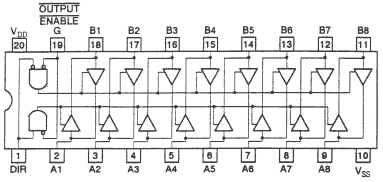
Interestingly, for a machine design that I understand focused on parts and cost reduction within TANDY, 1 part was added to the CPU’s data path along the memory bus, an addition that renders our previous work unusable, an addition that breaks the very idea of sharing the bus: the 74LS245 octal bus transceiver. Ironically, the ‘245 transceiver was designed to allow bus sharing. As the name suggests, it contains 8 logic elements, each able to pass one signal from the ‘A’ pin to the ‘B’ pin or vice versa, depending on the state of the “direction” pin. More importantly, when an “enable” pin is de-activated, the logic element effectively “removes” the signal from the pin on the IC. In the industry, the pin is said to be in high impedance mode or “Hi-Z” mode. Such pins are commonly called “tri-state” pins, as they can either output 0, 1, or Hi-Z. The mechanics vary, but the term implies the logic element effectively places such a large resistance in between the signal and the pin that the rest of the circuit can essential ignore or will have no awareness of the signal. The 8 elements, Hi-Z operation, and direction function fit the demands of an 8-bit CPU bidirectional data bus perfectly. We can’t blame the IC itself for this issue, so why does the inclusion of this IC in the Color Computer 3 design render bus sharing unusable?
Let’s peruse the CoCo3 schematic, located on page 103 (or 127 for PAL) of the TANDY Color Computer 3 Service Manual. A snippet is included below in Figure 2. The 74LS245 connects directly to the MC6809E CPU data bus, with the DIR line connected to the CPU R/W line. During normal operation, the CPU drives the ‘B’ lines during a write action, and the ‘245 reads those lines and drives the ‘A’ lines with the same value. On a read activity, the ‘245 reads the data bus ‘A’ lines and drives the ‘B’ lines with that value, which the CPU then reads on its data pins and processes.
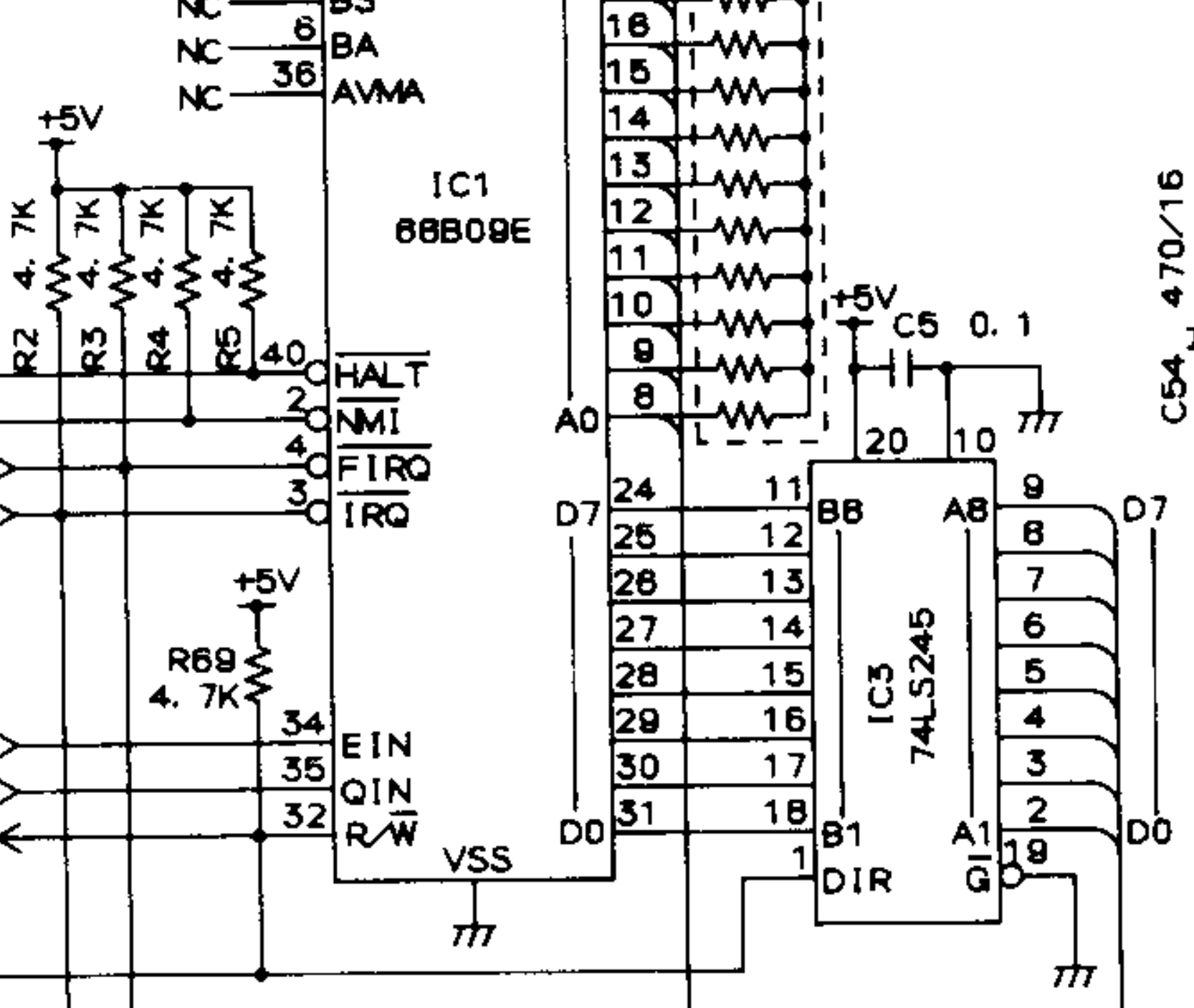
So far, so good. And, all works fine when we perform a DMA-based read action. After halting the CPU, The DMA engine places an address on the bus, and raises the R/W line to read data from memory, just like the CPU. Doing its part, the ‘245 transceiver pulls the data from the ‘A’ pins and places it on the ‘B’ pins, which are connected to the CPU. It’s a nice gesture, though unneeded, since the CPU isn’t running.
Writing, though, is where the issues arrive. Let’s run through the scenario. After halting the CPU, the DMA engine places an address on the address bus, places some data on the data bus, and pulls the R/W line low to signal a memory write. The ‘245, assuming the CPU is trying to write some data to memory, grabs the values on the ‘B’ pins and places the results on the ‘A’ pins, which are connected directly to the shared data bus. The first problem: The CPU is halted, so it is not outputting any data on the CPU data pins. The ‘245 is effectively pulling residual charge from the tri-stated CPU data bus, cleaning it up and driving the data bus. The second problem: Someone else is already driving the bus: the DMA engine. At the very least, the data bus represents an interdeterminate composite of the expected value from the DMA engine and the unknown value from the CPU data pins. More importantly (and more concerning), one output might be attempting to drive a data line low while the other tries to drive it high. In some sense, this is like connecting a battery’s positive post to its negative post. While the amperage involved is much lower, it’s no less damaging to the ICs.
Focus attention on pin 19 of the 74LS245, the “enable” pin, labeled “G”. (I have not yet been able to determine why “G” was used, maybe “gate”. Other versions of the IC use OE, which means “output enable”). Regardless of the name, the bar over the name indicates that it is “active low”. A logic zero (0) on the pin will enable the function. Ground the pin, and the data passes from A to B or B to A. Connect the pin to a “one” (1) signal and all transceiver channels switch into Hi-Z mode. Notice in Figure 2 that the enable line is connected to a symbol that just ends. That symbol is called “chassis ground”, representing a wire connected to a large sheet of metal (the “chassis” of old electronic equipment was made of metal). I won’t go into the specifics of various grounding options (signal ground, earth ground, and chassis ground), but we can all agree this pin is permanently tied to zero (0). Thus, the transceiver is permanently enabled. Good for the CPU, bad for DMA.
On previous Color Computer designs, the 74LS245 was not even included. I don’t know exactly why the functionality was added to the CoCo3, but we can theorize. While dedicated bus transceivers like the ‘245 clean up marginal signals, it’s highly doubtful that signals originating from the MC6809E showed any integrity loss. Bus transceivers like the 74LS245 can also act as “buffers”, protecting (in this case) the CPU from dangerous voltages or skipes on the data bus. Again, this seems dubious, since dangerous voltages on the address bus or other control lines could just as easily damage the CPU, and no buffers are placed on those lines. However, bus transceivers are also used to increase the “drive” capability of a signal. Think of the bus transceiver like an 8 channel amplifier. Each IC connected to the bus uses a bit of power, which must be supplied by the IC driving the bus. ICs thus often specify their drive characteristics in terms of Transistor to Transistor Logic (TTL) “load”, a current requirement of 1.6 milliampere (mA). A standard TTL IC input comprises one (1) TTL load, and a TTL output can typically drive ten (10) TTL loads (16mA). In electronics, this is called the “fanout” rating. Most ICs provide their fanout capability, and the MC6809E specifies a fanout capability of 4 LSTTL loads. A LSTTL (Low Power Schottky TTL), as the name suggests, requires less power than standard TTL. As such, an LSTTL load is equivalent to ¼ TTL load, or 0.4mA. Even if we simplify and consider everything on the CoCo3 data bus as requiring only 1 LSTTL load (0.4mA) each, the CoCo3 attaches 6 items besides the cartridge port and CPU to the databus, which exceeds the 4 LSTTL limit. For comparison, the CoCo1 attaches 5 items, again not including the CPU and the cartridge port. While the MC6809 can probably drive more than 4 LSTTL loads, and CMOS devices like the GIME probably consume less than 1 LSTTL of load, the ‘245 was most likely placed into the design to address this load issue. Now, some will ask, “But, what about the need to boost the drive on the address lines”? It turns out that the address lines are not connected to as many devices (excepting the cartridge port, most address lines only connect to GIME and the ROM, with A0,A1, and A5 signals connecting to 2 more devices).
We’ve determined the bus transceiver is designed to allow bus sharing, and our theory suggests it was a useful addition to the CoCo3 design. So, how should we proceed? As the title of this article suggests, the problem lies in a missing wire in the schematic. Such lines, called printed circuit board (PCB) traces or just traces, connect all of the IC pins in the CoCo3 design. As noted previously, we need one connected to the “enable” pin of the bus transceiver, one that will be zero (0) when the transceiver should be working, and one (1) when the transceiver should be turned off.
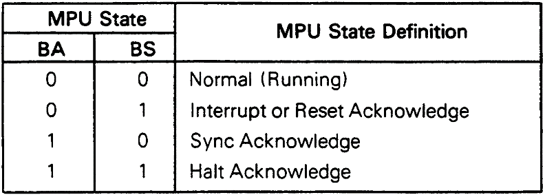
It turns out that the MC6809E CPU “BA” (Bus Available) line appears to offer the correct operation and polarity. When zero (0), the CPU is utilizing the bus, and while one (1), the bus is “available” for others. Tying the “enable” line to the CPU BA line should allow all existing functionality to continue while enabling CoCo3 DMA operation. That’s the good news. The bad news: adding this trace in some fashion requires hardware modification. Take heart, though, there are a few different ways to proceed.
For reference, let’s look at an NTSC CoCo3 PCB in Figure 4, showing the 74LS245 bus transceiver. You will notice the transceiver sits in between the CPU and the cartridge port (the PAL PCB is slightly different):
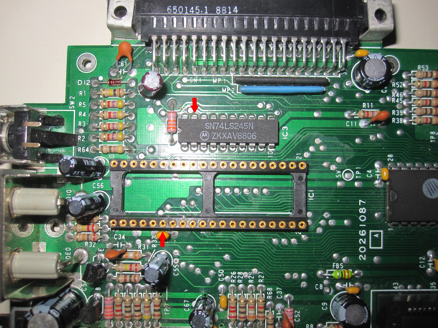
The “enable” pin on the 74LS245 has been denoted with the red arrow, as has the BA pin on the MC6809E (this particular CoCo3 has had the CPU removed and a socket installed).
NOTE: While testing suggests this modification will not adversely affect any current CoCo3 usage, more testing is needed to conclusively prove the point. The below instructions are designed for those who want to modify and confirm operation. Make these modifications at your own risk.
Option 1:
This option requires the least amount of work, but also looks the least pleasing. Simply snip the 74LS245 pin 19 at the spot where it goes into the PCB, bend it up off the PCB, and solder a small wire from it to pin 6 of the CPU. To return to stock, simply remove the wire, bend the pin down, and resolder to the stub in the PCB. Alternatively, desolder and replace the 74LS245.
Option 2:
This option looks neater, but does require cutting a trace.
For this option, remove the PCB from the case, remove the little retaining clips on the shield under the board, and locate pin 19 of the 74LS245. Cut the trace going to that pin, and then solder a wire from pin 19 to pin 6 of the CPU on the bottom of the PCB. To return to stock, unsolder the wire and create a small solder bridge over the cut trace.
Option 3:
This option requires the most work, but it is easiest to convert back to stock.
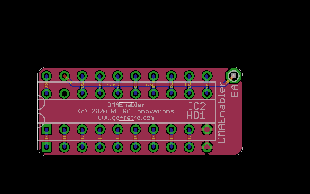
Desolder and socket the 74LS245. Build and populate the DMEnabler PCB shown below, installing the ‘245 into the adapter PCB and then installing the adapter into the CoCo3. Attach a test grabber lead to the BA pin on the adapter PCB and clip the test lead to pin 6 of the CPU. (Enterprising PCB designers could also create a dual-header PCB that fits in both the CPU and the 74LS245 sockets, removing the need for the test lead)
With one of these alterations, normal CoCo3 operation should continue as before, and DMA functionality will be enabled. As teased in last week’s article, with this modification in place, our test application now transfers data from the CoCo3 to external RAM and back:
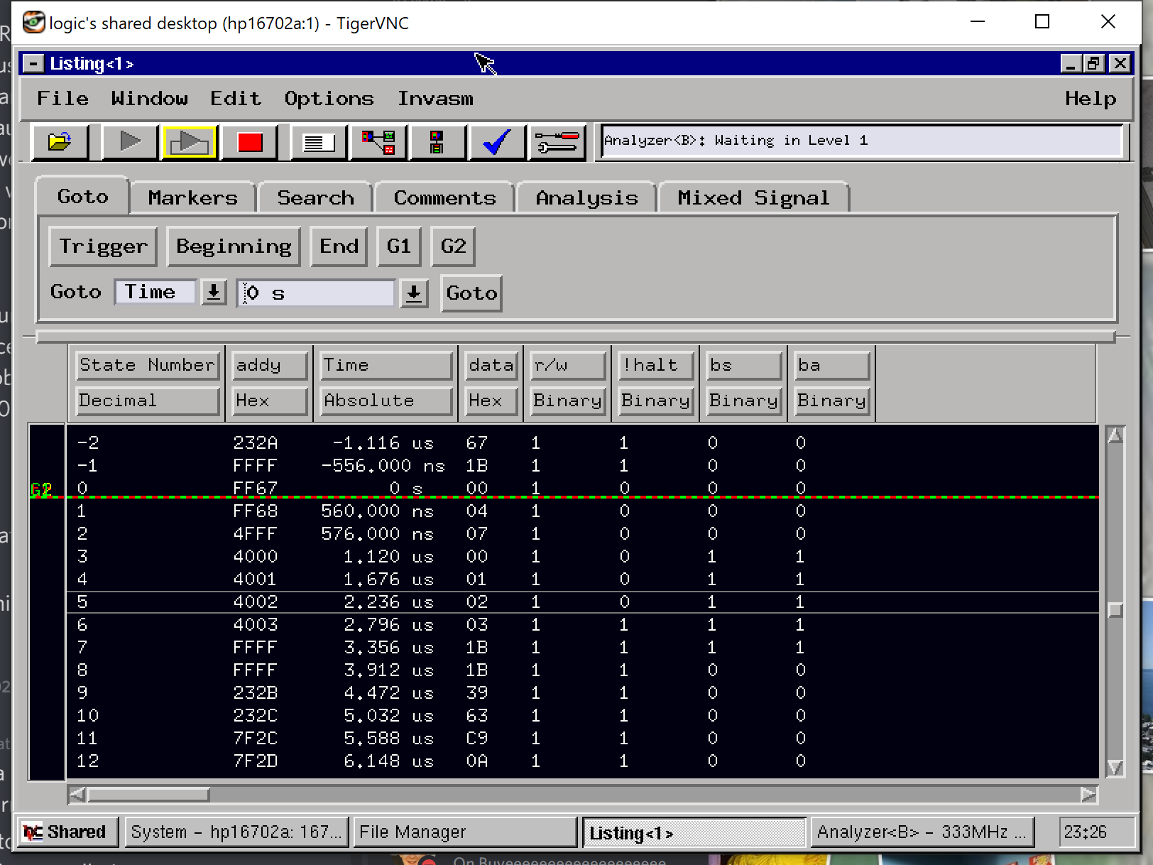
While running in FAST mode (poke &hffd9,0), we can see the double read of $ff67/68 trigger the DMA transfer, which then pulls data from $4000-$4003 at ~2MBps.
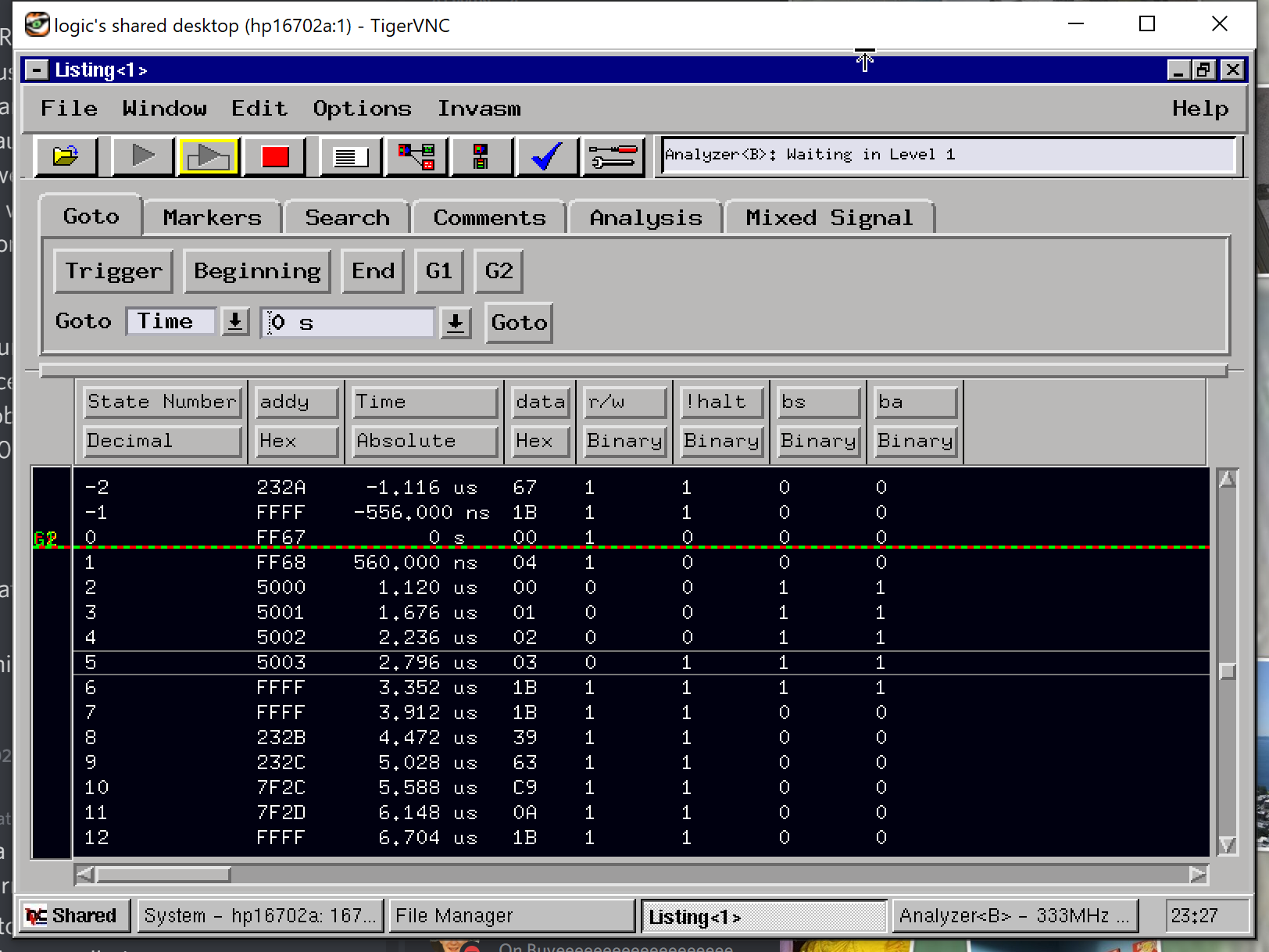
Going the other way, the two cycle $ff67/68 read triggers the engine to push our data to $5000-$5003, again at ~2MBps.
Given that the addition of a single PCB trace into the CoCo3 circuit board would have added no cost and that the inclusion of that trace appears to maintain full compatibility with earlier CoCo systems while also fully enable bus sharing, one can only assume TANDY did not foresee DMA or other bus sharing activities being needed on the cartridge bus or they did not care to support such functions. Alas, requiring a hardware modification to support CoCo3 bus sharing severely limits adoption of this technique. At this point, folks socketing their CPU to upgrade to the Hitachi 63C09 CPU could also start socketing the 74LS245 or otherwise asking this modification be performed, but the majority of CoCo3 units remain unable to utilize this DMA technique.
Still, one cannot help but wonder… What if there were a way to coax an unmodified CoCo3 into sharing the bus? 🙂