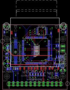
My plan to ship uIEC/SD units by end of June was evidently overly optimistic. It took longer than expected to modify the uIEC/SD PCB design, and the design had to be checked more thoroughly since I will not have time to assemble and test a sample before ordering the SMT stencil (a metal “mask” laid over the PCB that is used to force solder paste to only deposit on the exposed PCB pads) and a production PCB run. Thus, I am crossing my fingers that the redesign is correct. The new design looks very similar to the older, though I have designed the PCB to fit a small Hammond 1551 enclosure (the 2 half-present holes on the corners of the board).
At this point, I’ve moved the expected ship date to July 12, and alerted customers about the delay.